Download
1 / 15
150 likes | 291 Vues
Hall effect in pinned and sliding states of NbSe 3. A. Sinchenko , R. Chernikov , A. Ivanov MEPhI, Moscow P. Monceau, Th. Crozes Institut Neel, CNRS, Grenoble. Outline. Hall effect in CDW compounds. Motivation of studying of NbSe 3 .

E N D
Hall effect in pinned and sliding states of NbSe3 A. Sinchenko, R.Chernikov, A. Ivanov MEPhI, Moscow P. Monceau, Th. Crozes Institut Neel, CNRS, Grenoble
Outline • Hall effect in CDW compounds. Motivation of studying of NbSe3. • Hall effect in NbSe3 at low longitudinal electric field E<Et. Comparison with magnetoresistance. Two band model problems. • Hall effect in NbSe3 in sliding state of CDW. Hole and electron pockets: what is the difference? • Conclusion
Hall effect in NbSe3 (E<Et) NbSe3 in the Pierlse state –– semimetal ground state because small electron andhole pockets in the Fermi surface main contribution to the Hall effect from pockets carriers Hall voltage is quite unusual in NbSe3 below Tp2=59 K - strong non-linear magnetic field dependence which drives the Hall voltage through a negative minimum and then positive at higher fields. • Monceau and Ong (1978) reported that the zero-field-limit Hall constant changes sign from n-type to p-type at 15 K. • Explanation in the frame of a two-band model (Ong 1978) in which the difference in population (np-nn)= 31018 cm-3 below Tp2. What is correct? R.V. Coleman, et al, PRB, 1990
Hall effect in the compounds with a CDW. (E>Et) TaS3 S. Artemenko, et al, JETP Lett., 1984 K0.3MoO3 L. Forro, et. al, PRB, 1986 Does CDW give contribution to the Hall voltage? Explanation – CDW itself does not give contribution to the Hall voltage. Non linear Hall voltage is result of normal metal “back-flow” (S. Artemenko and F.Kruglov, (Sov. Phys. Solid State, 1984)
Hall effect in NbSe3 (E>Et) NbSe3 – G.X. Tesseme and N.P. Ong – CDW motion gives no visible contribution to the Hall effect. (PRB, 1981) “Back-flow” model predicts reduction of VH also in NbSe3 especially at the temperatures close to Tp. Where is back-flow?
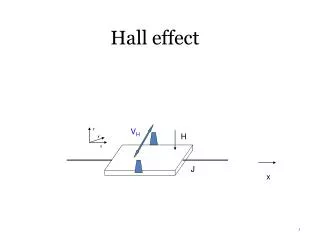
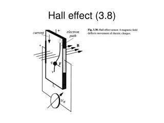
Experimental Two types of structure: • Evaporation of gold contacts • to the opposite faces of crystal 2. Preparation of Hall probes from the crystal itself In both cases the change in voltage on the Hall pairs of contacts [V1,3(+B)-V1,3(-B)]/2 or [V2,4(+B)-V2,4(-B)]/2 was taken to be equal to the Hall voltage, VH, and the sum [V1,3(+B)+V1,3(-B)]/2 or [V2,4(+B)+V2,4(-B)]/2 was taken as a longitudinal drop of voltage.
Experimental results (E<Et) At low electric field (E<<Et) the Hall voltage is linear function of current. CDW does not give the contribution to the electric transport. RH=VH/I 5K 35K RH is strongly magnetic field dependent and demonstrates the reversal of the Hall constant sign at all temperatures
Comparison with magnetoresistance maximum dR/dB at B=B0 B<B0 MR ~ B2 B>B0 MR ~ B
Comparison with magnetoresistance B0=Bzc? Electron and hole pockets demonstrate quite different behavior in magnetic field: electrons: MR~B2 holes: MR~B
MR~B2 - usual MR~B - unusual Quantum linear magnetoresistance ? Conditions (Abrikosov, 1999): In the case NbSe3 n ~1017cm-3 and m*~ 10-2me Two band model: n ~1018cm-3 and m*=0.24me 1 – high -T CDW 2 - low - T CDW 3 - ? NbSe3 – 3 types of chains heavy electrons + small hole pockets because non-perfect nesting of low-T CDW (m*~ 10-2me) Correlation with ARPES data (J. Schafer et al, PRL, 2003)
Experimental results (E>Et) 30 K A first step – what is the Et(B) dependence? Threshold electric field is practically Independent on magnetic field at T>25 K. Experimental results – above 25 K
30 K Second type of Hall contacts (litography) First type of Hall contacts (evaporated) In both cases – strong influence of CDW motion on the Hall voltage. Three possibility to explain: 1. Field generation model – CDW generates normal carriers 2. CDW motion deforms electron or hole pockets. 3. “back-flow” model if CDW interacts with one type of carriers only (with light holes?).
To make this effect more pronounce, we determine the difference δVH=VH-Vlin The last term is the linear Hall voltage dependence observed at low electric field below the threshold. 30 K Below Et – visible deviation of the Hall voltage from linear dependence. Position of this deviations coincides with corresponding singularities in IV-curve. Most probably – this effect is attributed by the local CDW deformations.
Temperarure evolution Deviation of the Hall voltage from linear `dependence decreases with the temperature increase. δ VH=A·exp(-T/T0) T0=3.4 K
conclusion 1. Hall voltage, VH, changes sign in a wide temperature range and the magnetic field for which VH crosses zero is temperature dependent. The two band model needs corrections. 2. Electron and hole pockets demonstrate qualitatively different magnetoresistance behavior. 3. in high magnetic field the CDW motion changes significantly the Hall voltage at all temperatures below Tp2, that can not be explained in the frame of "back-flow" model. 4. Our results indicate that the CDW in the sliding state interacts differently with electrons and holes leading strong change in the normal carriers concentration at Et. Thanks to S. Brazovskii and Yu. Latyshev