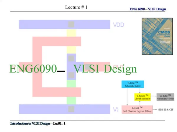
VLSI DESIGN DOMAIN
VLSI DESIGN DOMAIN. Practical application of VLSI Design?. INTRODUCTION. Systems based on Magnetically controlled switches Vacuum Tubes Analog Digital. HISTORICAL PERSPECTIVE. 1930 - O.Heil and Lilienfeld – FET 1947 – Bardeen, Brattain and Shockley, AT & T Bell Labs, - BJT

VLSI DESIGN DOMAIN
E N D
Presentation Transcript
VLSI DESIGN DOMAIN • Practical application of VLSI Design?
INTRODUCTION • Systems based on Magnetically controlled switches • Vacuum Tubes • Analog • Digital
HISTORICAL PERSPECTIVE • 1930 - O.Heil and Lilienfeld – FET • 1947 – Bardeen, Brattain and Shockley, AT & T Bell Labs, - BJT • 1958 – Jack Kilby, Texas Instruments, Hybrid IC • Jack Kilby was awarded the year 2000 Nobel prize
LEVEL OF INTEGRATION Level of Number Typical Integration of Gates Applications SSI 1-10 Basic Gates MSI 10-100 Counters,Decoder, Encoder LSI 100-1000 Memories, ADC/DAC VLSI 1000-10,000 MPU’s ULSI 10,000-100,000 DSP, DEC ALPHA
Silicon in 2010 Die Area: 2.5x2.5 cm Voltage: 0.6 V Technology: 0.07 m
TERMINOLOGY • Manufacturing Lead Time(Turnaround Time) – The time it takes to make an IC excluding the design time. • Integrated Circuit – Combination of circuit elements inseparably associated on or within a substrate. • Substrate – Supporting material. • Monolithic IC – An IC whose elements are formed on or within a substrate. • Hybrid IC – Consists of a combination of two or more ICs or an IC with some discrete components.
TERMINOLOGY • Wafer(Slice) – Contains many ICs. Circular in nature. Diameter – 4, 5, or 6 inches. • Chip(die or bar) – Repeated ICs on a wafer. • Test Plug(Process Control Bar Process Control Monitor) - Special Chip Used to monitor the process parameters of the technology.Used to derive the timing models-Wafer can be discarded.
TERMINOLOGY • Defect Density - Lethal defects per cm2 • Yield - Yield = No. of Good Chips on a Wafer/Total Number of Chips • Utilization Factor - Utilization Factor = Used Chip Area/Total Chip Area • SOC- System On Chip
Intrinsic Si Ideal crystal structure Valance 4 Almost no free carriers Almost no conduction SEMICONDUCTOR PHYSICS
Doping with valance 5 atoms (Phosphor, Arsenic) introduces “Loose electrons” Electron donor Conductivity depends on doping level SEMICONDUCTOR PHYSICS
Doping with valance 3 atoms (Boron) introduces “Loose Holes” Electron acceptors Hole conductivity lower than electron conductivity SEMICONDUCTOR PHYSICS