Overview of SPI Protocol and RF Control in SDR Systems at Rutgers University
This document presents an overview of the Serial Peripheral Interface (SPI) protocol used in controlling RF modules in Software Defined Radio (SDR) systems at Rutgers University. Highlighting the operation in master/slave mode, it details the clock signals, data transmission methods, and configuration requirements, including clock polarity and phase settings. The OCRP RF Control block enables multi-module control and specifies different configurations for shared SPI buses. These insights are crucial for understanding RF system architecture and enhancing communication efficiency among components.


Overview of SPI Protocol and RF Control in SDR Systems at Rutgers University
E N D
Presentation Transcript
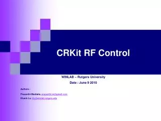
CRKit RF Control WINLAB – Rutgers University Date : June 9 2010 Authors : Prasanthi Maddala, prasanthi.m@gmail.com Khanh Le, kle@winlab.rutgers.edu
SPI – Serial Peripheral Interface Synchronous serial data link standard. Operates in master/slave mode. SPI specifies 4 logic signals SCLK — Serial Clock (output from master) MOSI/SIMO — Master Output, Slave Input (output from master) MISO/SOMI — Master Input, Slave Output (output from slave) SS — Slave Select (active low; output from master) Some SPI slave devices do not have a data output port (No MISO) and a few devices use a bidirectional data port (MOSI/MISO). Data Transmission - Master configures the clock; uses a frequency < max. freq supported by the slave - Pulls the slave select low - During each clock cycle the Master sends a bit on MOSI and slave sends a bit on MISO – not all transmissions result in meaningful rd/wr s. Clock polarity and phase - In addition to setting the clock frequency, the master must also configure the clock polarity(cpol) and phase(cpha) with respect to the data.
SPI (contd.) • At CPOL=0 base value of the clock is zero • For CPHA=0 (first edge), data is read on the clock's rising edge and data is changed on a falling edge • For CPHA=1 (second edge), data is read on the clock's falling edge and data is changed on a rising edge. • At CPOL=1 the base value of the clock is one (inversion of CPOL=0) • For CPHA=0, data is read on clock's falling edge and data is changed on a rising edge. • For CPHA=1, data is read on clock's rising edge and data is changed on a falling edge. • This timing applies to both the master and the slave device.
Range Of RF Boards *Each “part” of an RF module has its own SPI data bus
OCRP RF Control (R3/ocrp_rf_ctl.vhd) OCRP RF Control block supports up to 4 RF modules (SDR/ SDR with FreeBo/ WDR/XDR(?)) Generics: RF_BOARD – SDR/SDRwithFreeBo/WDR/XDR NO_OF_RF_CARDS - 1 or 2 for SDR, 1 for SDR with FreeBo(eSDR), 1-4 for WDR, 1-4 for XDR SPI_PER_CARD_SHARED (TRUE by default) - User can choose to share an spi master among different spi slaves, even when they have independent SPI buses. In SDR, DiBo and WiBo have independent SPI buses. When SPI_PER_CARD_SHARED = TRUE, a single SPI master is used to generate the SPI signals, that are routed to the required bus, using an intermediate block. - TRUE or FALSE for SDR, SDRwith FreeBo(eSDR),always TRUE for WDR, XDR Made up of OCRP SPI blocks (up to 4), each of which is controlled through an RMAP interface (RMAP Inf x) as shown above.
SPI Devices on SDR Antenna Switches are controlled from the common RMAP directly just like the LEDs – they don’t go through the RF control block
RF Control for SDR OCRP RF CTL (RF_BOARD=SDR, NO_OF_RF_CARDS=1, SPI_PER_CARD_SHARED=TRUE) OCRP RF CTL (RF_BOARD=SDR, NO_OF_RF_CARDS=2, SPI_PER_CARD_SHARED=TRUE) OCRP RF CTL (RF_BOARD=SDR, NO_OF_RF_CARDS=1, SPI_PER_CARD_SHARED=FALSE) OCRP RF CTL (RF_BOARD=SDR, NO_OF_RF_CARDS=2, SPI_PER_CARD_SHARED=FALSE) By default and preferably SPI_PER_CARD_SHARED = TRUE
RF Control for SDR(Contd.) Generic SPI SLAVE_SEL_ENCODED - FALSE NO_OF_SLAVE_SEL_OUTPUTS – 1 DELAY_TO_SLAVE – 1 (since SDR RF inf involves a delay of 1 sclk cycle)
RF Control for SDR(Contd.) Generic SPI (OCRP SPI – WIBO) SLAVE_SEL_ENCODED – FALSE NO_OF_SLAVE_SEL_OUTPUTS – 2 DELAY_TO_SLAVE – 0 Generic SPI (OCRP SPI – DIBO) SLAVE_SEL_ENCODED – FALSE NO_OF_SLAVE_SEL_OUTPUTS – 1 DELAY_TO_SLAVE – 0
Generic SPI Generics MAX_SPI_CYCLE_LEN (40 for OCRP) MAX_SPI_CYCLE_LEN_BITS (6 for OCRP) NO_OF_SLAVE_SEL_INPUT_BITS (4 for OCRP) SLAVE_SEL_ENCODED (depends on RF) NO_OF_SLAVE_SEL_OUTPUTS (depends on RF) DELAY_TO_SLAVE (depends on RF) - 0 if the SPI master core is directly connected to the slave. If its output is being processed before connecting to the slave, specify the delay involved in terms of sclk cycles.
RMAP settings for SDR(rmap_cmn_ctl.xls) *freq_div = 3. this gives sclk of 12.5 MHz when i_clk i.e., the system clock is 100 MHz ** AD9862 supports two word write, in which case cycle_len = 24. We always use single word write. So, cycle_len = 16 Since the spi_config register remains the same for all the devices on SDR, just write it once.
RF Control for eSDR OCRP RF CTL (RF_BOARD=eSDR, NO_OF_RF_CARDS=1, SPI_PER_CARD_SHARED=TRUE) OCRP RF CTL (RF_BOARD=eSDR, NO_OF_RF_CARDS=1, SPI_PER_CARD_SHARED=FALSE) By default and preferably SPI_PER_CARD_SHARED = TRUE
RF Control for eSDR(Contd.) Generic SPI SLAVE_SEL_ENCODED - FALSE NO_OF_SLAVE_SEL_OUTPUTS – 1 DELAY_TO_SLAVE – 1 (since eSDR RF inf involves a delay of 1 sclk cycle)
RF Control for eSDR(Contd.) Generic SPI (OCRP SPI – WIBO) SLAVE_SEL_ENCODED – FALSE NO_OF_SLAVE_SEL_OUTPUTS – 2 DELAY_TO_SLAVE – 0 Generic SPI (OCRP SPI – DIBO) SLAVE_SEL_ENCODED – FALSE NO_OF_SLAVE_SEL_OUTPUTS – 1 DELAY_TO_SLAVE – 0 Generic SPI (OCRP SPI – FreeBo) SLAVE_SEL_ENCODED – FALSE NO_OF_SLAVE_SEL_OUTPUTS – 3 DELAY_TO_SLAVE – 0
RMAP settings for eSDR(rmap_cmn_ctl.xls) *freq_div = 3. this gives sclk of 12.5 MHz when i_clk i.e., the system clock is 100 MHz ** AD9862 supports two word write, in which case cycle_len = 24. We always use single word write. So, cycle_len = 16 Since the spi_config register remains the same for all the devices on SDR, just write it once.
RF Control for WDR OCRP RF CTL (RF_BOARD=WDR, NO_OF_RF_CARDS=n (n = 1/2/3/4), SPI_PER_CARD_SHARED= x ) By default and preferably SPI_PER_CARD_SHARED = TRUE
RF Control for WDR(Contd.) Generic SPI SLAVE_SEL_ENCODED - TRUE NO_OF_SLAVE_SEL_OUTPUTS – 4 DELAY_TO_SLAVE – 0