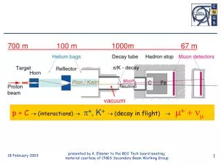
Vacuum
Principles for Formation of Transversely Modulated Heterophase Nanostructures Hugh A. Bruck , University of Maryland, DMR 0907122.

Vacuum
E N D
Presentation Transcript
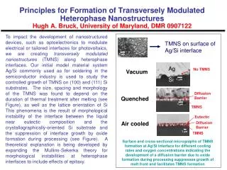
Principles for Formation of Transversely Modulated Heterophase NanostructuresHugh A. Bruck, University of Maryland, DMR 0907122 To impact the development of nanostructured devices, such as optoelectronics to modulate electrical or tailored interfaces for photovoltaics, we are creating transversely modulated nanostructures (TMNS) along heterophase interfaces. Our initial model material system Ag/Si commonly used as for soldering in the semiconductor industry is used to study the controlled growth of TMNS on (100) and (111) Si substrates. The size, spacing and morphology of the TMNS was found to depend on the duration of thermal treatment after melting (see Figure), as well as the lattice orientation of Si This phenomena is the result of morphological instability of the interface between the liquid near eutectic composition and the crystallographically-oriented Si substrate and the suppression of interface growth by oxide formation during processing (see Figure). A theoretical explanation is being developed by expanding the Mullins-Sekerka theory for morphological instabilities at heterophase interfaces to include effects of epitaxy. TMNS on surface of Ag/Si interface 1 mm Ag No TMNS Vacuum Si 1 mm Diffusion Barrier Quenched 1 mm TMNS Eutectic Air cooled Diffusion Barrier 1 mm TMNS Surface and cross-sectional micrographs of TMNS formation at Ag/Si interface for different cooling rates and oxygen concentrations indicating the development of a diffusion barrier due to oxide formation during processing suppresses growth of melt front and facilitates TMNS formation
Principles for Formation of Transversely Modulated Heterophase NanostructuresHugh A. Bruck, University of Maryland, DMR 0907122 2.) 1.) Transversely modulated nanostructures (TMNS) have been recently discovered in BiFeO3 epitaxial ferroelectric films, which provide large electromechanical responses. The analysis of these nanostructures provides the opportunity to develop and verify the general principle of formation and evolution of TMNS. In good agreement with experiment, the concept of elastic domains has been used to find the equilibrium nanostructure of alternating rhombohedral-tetragonal (R-T) phases forming heterophasepolydomains, including the crystallographic orientation of domain interface, their relative fractions, and the monoclinic distortions of phases. It is shown that stability of the structure and its evolution is determined by a competition between the indirect and the direct elastic interdomain interactions. Changing substrates, substrate orientations and relative substrate thickness in multilayer structures enables one to modify indirect interaction to control heterophase film structure and optimize its field (eg. stress) induced response. 1.) Predicted R-T polydomain structure on substrate. 2.) Misfits εR and εT of R and T phases with substrate determine elastic indirect interaction. Misfit ε0between the phases determine direct interaction. 3.) 3.) Free energies of phases and domain fraction αas a function of misfit. The point εscorresponds to a substrate with given lattice parameter.
Principles for Formation of Transversely Modulated Heterogeneous NanostructuresHugh A. Bruck, University of Maryland, DMR 0907122 As part of this effort, we have developed new educational curriculum. Materials science and engineering principles for epitaxial control of nanostructure formation as the basis for TMNS have been discussed during a lecture course on Thermodynamics in the Materials Science Department and in a lecture course on Materials by Design in Mechanical Engineering. Two undergraduate students, Mr. Josh Balsam and Mr. BowoAkinlabi-Oladimeji (underrepresented minority), a graduate student, Mr. Brad Boyerinas, and a post-doc, Dr. Daniel Cole, have been actively involved with the preparation of the Ag films on single crystal Si substrates in the DC magnetron sputtering machine. They have also been learning about the operation of the nanoindenter, SEM, and AFM used to characterize TMNS at UMD, NIST-Gaithersburg, and Sandia Livermore National Laboratory (Top) Slide from lecture on TMNS presented in Materials by Design course, and (right) Mr. Brad Boyerinas (PhD student) works with Mr. BowoAkinlabi-Oladimeji (UG underrepresented student) using the AFM to image TMNS films

