Download
1 / 38
880 likes | 1.58k Vues
First lecture, Mar. 4th, 2014. CC512 Introduction to Materials Science and Engineering Name of the Instructor : Taek Dong Lee (Professor Emeritus) ( 이택동 , 李 宅 東 ) Tel: (Office) : 350-3390, (CP) : 019-449-7267 Office W1-1 Rm 2316

E N D
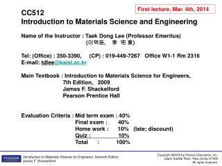
First lecture, Mar. 4th, 2014 CC512 Introduction to Materials Science and Engineering Name of the Instructor : TaekDong Lee (Professor Emeritus) (이택동, 李 宅 東) Tel: (Office) : 350-3390, (CP) : 019-449-7267 Office W1-1 Rm 2316 E-mail: tdlee@kaist.ac.kr Main Textbook : Introduction to Materials Science for Engineers, 7th Edition, 2009 James F. Shackelford Pearson Prentice Hall Evaluation Criteria : Mid term exam : 40% Final exam : 40% Home work : 10% (late; discount) Quiz : 10% Total : 100%
Lecture Time Schedule : Every Tuesdays and Thursdays 13:00 ~ 14:30 Room : 211 (E 11) Teaching Assistance(s) : Mr. Eun-Shin Sohn e-mail : sohnejgood@kaist.ac.kr Lab. T.3380 : CP : 010-9210-1349 Mr. Byungil Lee e-mail : polaris89@kaist.ac.kr Lab. T. 3380: CP : 010-9797-4182
Lecture Schedule for the SpringSemester, 2014 1st Week Mar. 4, Ch. 1; Materials for Engineering Mar. 6, Ch.2: Atomic Bonding 2nd Week Mar. 11, Ch. 3; Crystalline Structure-Perfection Mar. 13, Ch.3: Crystalline Structure-Perfection 3rd Week Mar. 18, Ch 4; Crystal Defects and NoncrystallineStructure Mar. 20, Ch 4; Crystal Defects and NoncrystallineStructure 4th Week Mar.25, Ch.4; Crystal Defects and Noncrystalline Structure Mar.27, Ch. 5; Diffusion 5th Week April 1, Ch. 5; Diffusion April 3, Ch .6; Mechanical Behavior 6th Week April 8, Ch 6; Mechanical Behavior April 10, Ch 6; Mechanical Behavior
7th Week April 15 ,Ch 7; Thermal Behavior April 17, Ch 8; Failure Analysis and Prevention 8th Week April 22 or April 24 , Mid-term exam. 9th Week April 29, Ch 9; Phase Diagrams-Equilibrium Microstructural Development May 1, Ch 9; Phase Diagrams-Equilibrium Microstructural Development 10th Week May 6, Holyday May 8, Ch 10; Kinetics-Heat Treatment
11th Week May 13, Ch 10; Kinetics-Heat Treatment May 15, Ch 11; Structural- Metals, Ceramics and Glasses 12th Week May 20, Ch 12; Structural Materials - Polymers May 22, Ch 12; Polymers, Composites 13th Week May 27, Ch 12; Composites May 29, Ch13; Electronic Materials 14th Week Jun 3, Ch 13; Electronic Materials Jun 5, Ch 13; Electronic Materials
15th Week Jun 10, Ch 13; Insulators, Semiconductors Jun 12, Ch 13; Semiconductors ?, Ch 14; Materials in Engineering Design Environmental Degradation 16th Week ; Jun 17 or Jun 19: Final Exams
CC512 Introduction to Materials Science and Engineering Lecture note is found at : http://mse.kaist.ac.kr BBS → CC512
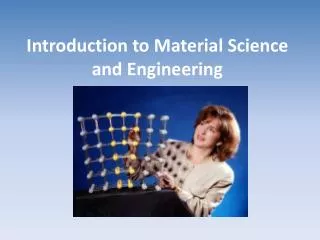
Introduction to the Course of Lecture : This lecture aims to make non-materials scientists know “what are the materials” and “how they can be used” for scientific research and engineering applications, onthe basis of the introduction level. Therefore, this lecture presents the structures and properties of materials, their origins, and the way they enter the engineering design. To meet the aims, the lecture deals with physical properties, mechanical characteristics, thermal behavior, electrical, magnetic and optical response, durability, processing, and the way it influences properties, and environmental issues.
Chapter1Materials for Engineering 1.1 The Material World 1.2 Materials Science and Engineering 1.3 Six Materials That Changed Your World 1.4 Processing and Selecting Materials 1.5 Looking at Materials by Power of Ten
1.1 The Materials World (Or human history in terms of the materials used) Materials we use define our social relationship and economic quality. The materials of the earlier human were probably for tools and weapons. In fact, the most popular way of naming the era of human civilization is in terms of materials from which these tools and weapons were made. The stone age : Starts from 2.5 million years ago. (Also, wood and animal fur) The pottery age: Before 4,000BC,domestic vessels were made and glass artifacts have been traced back to 4,000BC The copper age : It is estimated between roughly 4,000BC ~ 3,000BC. The bronze age : The period from 2,000BC to 1,000BC. Better quality of tools and weapons with the alloy of Cu-Sn. The iron age : The period from 1,000BC to 1BC. By 500BC, iron alloys had largely replaced bronze for tool and weapon making in Europe. The plastic age : Not officially referred but from second half of the 20th century, modern culture is supported by plastic. The silicon age : Another name of the same period of the plastic age during which silicon technology brought big revolution of computer. See Fig. 1.1 in next slide.
Figure 1.1The evolution of engineering materials with time. Note the highly nonlinear scale. (From M. F. Ashby, Materials Selection in Mechanical Design, 2nd ed., Butterworth-Heinemann, Oxford, 1999.) Increasing demand of not only high quality metallic alloys but non-metallic materials. WW II
1.2 Materials Science and Engineering The term of “Materials Science and Engineering” have been called in the general branch engineering from 1960s, (in Korea from 1970s, KAIST). Before this period, it was called Metallurgy or Metallurgical, and Ceramic Engineering. Because of the WW II and the space program, in addition to metals, the MSE has grownto include contributions from many traditional fields including metallurgy, ceramic engineering, polymer chemistry, solid state physics and physical chemistry. The word “science” covers the fundamentals of structure, classification, and properties, introduced in Ch 2 ~ Ch. 10. The word “materials” deals with five types of structural materials and electronic materials (semiconductors), in Ch. 11 ~ Ch. 13. The word “engineering” describes the key aspects of the selection of the right materials for the right job, explained in Ch. 14.
1.3 Six Materials That Changed Our World Six categories that encompass the materials available to practicingengineers : 1). Metals (crystalline materials, metallic bonding) 2). Ceramics (crystalline materials, ionic bonding) 3). Glasses (mainly non-crystalline materials, ionic bond) 4). Polymers (non-crystalline materials, covalent bonding) 5). Composites (mixture of above materials) 6). Semiconductors (unique electrical conducting behavior)
➀. Introducing Metals – steel bridges “Metals” give impressions of “structural steels”. Figure 1.2The Golden Gate Bridge north of San Francisco, California, is one of the most famous and most beautiful examples of a steel bridge. Metallic Materials have : 1). High strength and formability 2). Ductility (plastic deformation) Most of the bridges and high rising buildings are constructed with steels. Suspension bridge (현수교) Golden Gate Bridge, connecting San Francisco and Martin County, opened on May 27, 1937, as the longest suspension bridge of 2,737 meters.
Figure 1.3The Sundial Bridge in Redding, California is a modern masterpiece of bridge design. Another beautiful example of steel construction : the Redding Bride is a 66 meter pedestrian walkway.
Incheon Bridge (6 lanes) : Songdo – Incheon Int’l Airport Total length : 21.38㎞, Length over the sea : 12.12㎞ 주탑 높이는 63빌딩(249m)과 비슷한 230.5m The length between towers :800m World 5th longest cabled bridge (사장교) 진도 7의 지진이나 초속 72m의 강풍에도 견딜 수 있고, 10만t급 배가 충돌해도 안전
106-23=83 Figure 1.4Periodic table of the elements. Those elements that are inherently metallic in nature are shown in color. The shaded elements are inherently metallic and bases of the various engineering alloys, from Fe, Al, Mg, Ti, Ni, Zn, Cu and etc. (Si and Ge are not included in metallic group in this classification. Cf. see ceramics shown later.) 21/41
➁. Introducing Ceramics : (Lucalox lamp, See next slide, Fig 1.6) Metal oxides, MxOy, are no longer metals but called Ceramics. Ceramics have the properties ; ➊. Chemically stable ➋. Very high melting point Figure 1.5 Some common ceramics for traditional engineering applications. These miscellaneous parts with characteristic resistance to damage by high temperatures and corrosive environments are used in a variety of furnaces and chemical processing systems. } refractory ➌. high strength but very brittle Used in high temperature, corrosive environments, various furnaces, chemical processing systems. Example : Al2O3 (alumina), Mpt. = 2020oC, transparent, becomes translucent with impurity. Can be used for engine in replace of metal? Ceramics are eliminated from structural use because of its severe brittleness.
Arc tube made of translucent alumina Figure 1.6High-temperature sodium vapor lamp made possible by use of a translucent Al2O3 cylinder for containing the sodium vapor. (Note that the Al2O3cylinder is inside the exterior glass envelope.) Lucalox lamps (GE trade name) : High Pressure Sodium High Intensity Discharge Lamp for streetlights. High pressure sodium lamps are quite efficient—about 100 lm/W —when measured for photopic lighting conditions. They have been widely used for outdoor lighting such as streetlights and security lighting. Understanding the change in human color vision sensitivity from photopic to mesopic and scotopic is essential for proper planning when designing lighting for roads. (lm=lumen, for general electric lamps; 10 lm/W, for LED lamps; 100 lm/W)
Diagram of a high pressure sodium lamp. Because of the extremely high chemical activity of the high pressure sodium arc, the arc tube is typically made of translucent aluminium oxide. This construction led General Electric to use the tradename "Lucalox" for their line of high-pressure sodium lamps. Theory of operation An amalgam of metallic sodium and mercury lies at the coolest part of the lamp and provides the sodium and mercury vapor in which the arc is drawn. The temperature of the amalgam is determined to a great extent by lamp power. The higher the lamp power, the higher will be the amalgam temperature. The higher the temperature of the amalgam, the higher will be the mercury and sodium vapor pressures in the lamp. An increase in these metal pressures will cause a decrease in the electrical resistance of the lamp.
Sintering of ceramics and its effects : Commercial ceramics are frequently made by heating (sintering) crystalline powders to high temperatures until a relatively strong and dense productsare produced. Traditional ceramics made in this way contains a substantial amount of residual porosity which makes it opaque, low density and so low impact strength. Reduction in porosity is very important to improve the quality of ceramics and is achieved by adding a small amount of impurity (for ex. 0.1% MgO, glass forming component) which makes high-temperature densification process for the Al2O3 powder to make dense product during sintering. With this densification by impurity of MgO, the Al2O3 becomes translucent which can be used for the high-temperature sodium vapor lamp, shown in Figure 1.6.
Nonmetallic ceramic forming elements Metallic Elements Figure 1.7 Periodic table with ceramic compounds indicated by a combination of one or more metallic elements (in light color) with one or more nonmetallic elements (in dark color). Note that elements silicon (Si) and germanium (Ge) are included with the metals in this figure but were not included in the periodic table shown in Figure 1.4. They are included here because, in elemental form, Si and Ge behave as semiconductors (Figure 1.16). Elemental tin (Sn) can be either a metal or a semiconductor, depending on its crystalline structure. Ceramics are usually oxides. However, silicon nitride (Si3N4) is an important nonoxide ceramic used in a variety of structural applications. Some ceramics are chemical compounds made up of one of the five nonmetallic materials, C, N, O, P or S, shaded with dark blue color in figure 1.7. Very many variety of ceramic materials can be formed. (C, N, P, S are forming none-oxide ceramics with metallic elements.) (Now, Si and Ge are included as metallic elements in this classification, because they form ceramics.)
➂. Introducing Glasses – optical fibers Different from metals and ceramics, glasses are noncrystalline materials. See the figure shown below. Crystalline ceramics Noncrystalline glass Figure 1.8Schematic comparison of the atomic-scale structure of (a) a ceramic (crystalline) and (b) a glass (noncrystalline). (Nonmetal atom : o, metal atom : ●)
Glasses continued The general term for noncrystalline solids with composition comparable to those of crystalline ceramics is GLASS. Figure 1.9Some common silicate glasses for engineering applications. (Transparent and chemically stale) Most common glasses are silicates; ordinary window glass is approximately 72% silica (Si02) by weight, with the balance of materials being primarily sodium oxide (Na2O) and calcium oxide (CaO). Properties : transmit visible light as well as ultraviolet and infrared radiation, chemical inertness, and brittleness.
Glasses continued A major revolution in the field of telecommunication has occurred with the transition from traditional metal cable to optical glass fibers. Figure 1.10The small cable on the right contains 144 glass fibers and can carry more than three times as many telephone conversations as the traditional (and much larger) copper-wire cable on the left. Alexander Graham Bell first tried to transmit voice over a beam of light of several hundreds meters after his invention of the telephone. Nearly a century later, large-scale application could be possible by the invention of the laser in 1960. Nowadays, telephone conversations and any other form of digital data can be transmitted as laser light pulses rather than as the electrical signals used in copper cables, Glass fibers are excellent examples of PHOTONIC MATERIALS, in which signal transmission occurs by photons rather than by the electrons of electronic materials.
④. Introducing Polymers – Nylon parachutes Polymers brought major impact of modern engineering technology on everyday life. Figure 1.11Miscellaneous internal parts of a parking meter are made of an acetal polymer. Engineered polymers are typically inexpensive and are characterized by ease of formation and adequate structural properties. Plastics is an alternative name of polymers because of their extensive formability during fabrication, and they are synthetic (human-made) materials which represent a special branch of organic chemistry. Polymer is very attractive with its lightweight and low-cost. Polymers are long-chain molecules composed of many (100s to 1,000s) “mers” bonded together. Some examples of inexpensive, functional polymer products are shown in figure 1.11.
Polymers continued Figure 1.12Periodic table with the elements associated with commercial polymers in color. Small number of elements (6 elements) are involved for the formation of commercial polymers and most of polymers are simply compounds of hydrogen and carbon. Some other polymers contain oxygen (e.g., acrylics), nitrogen (nylon), fluorine (fluoroplastics) and silicon (silicones).
Polymers continued Nylon is a member of the family of synthetic polymers known as polyamides invented in 1935 at the DuPont Co. Nylon was the first commercially successful polymer and was initially used as bristles in toothbrushes (1938) followed by the highly popular use as an alternative to silk stockings (1940), and nylon became the focus of an intensive effort during the early stages of WWII to replace the diminishing supply of Asian silk for parachutes and other military supplies. (beginning of “INSTRON”) Today nylon remains a popular fiber material, but it is also widely used in solid form for application such as gears and bearings. Figure 1.13Since its developm-ent during W W II, nylon fabric remains the most popular material of choice for parachute designs.
⑤. Introducing Composites - Kevlar - reinforced tires Composites are another set of materials made up of some combination of individual materials from the previous categories materials with their own bonding characteristics. The excellent example is fiberglass, the composite of glass fibers embedded in a polymer matrix (Fig. 1.14). Characteristic of good composites is producing a product that is superior to either of the components separately that is it has both high strength and excellent flexibility. Figure 1.14Example of a fiberglass composite composed of microscopic-scale reinforcing glass fibers in a polymer matrix.
Composites continued Figure 1.15Kevlar reinforcement is a popular application in modern high- performance tires. In this case, the durability of sidewall reinforcement is tested along concrete ridges at a proving ground track. Kevlar fiber reinforcements provide significant advances over traditional fibers for polymer-matrix composites. Kevlar is a DuPont trade name for poly p-phenyleneterephthalamide (PPD-T), a para-aramid fiber. Also, at the same time, substantial progress has been made in developing new polymer matrices, such as PEEK and PPS which have the advantages of increased toughness and recyclability. Therefore, Kevlar-reinforced polymers to be composites are used in pressure vessels and tires. The strength-to-weight ratio of Kevlar is five times higher than that of structural steels.
⑥. Introducing Semiconductors – Silicon chips Figure 1.16Periodic table with the elemental semiconductors in dark color (Si, Ge, Sn) and those elements that form semiconducting compounds in light color. The semiconducting compounds are composed of pairs of elements from columns III and V (e.g., GaAs) or from columns II and VI (e.g., CdS). A relatively small group of elements shaded in the above figure 1.16 and their compounds has an important electrical property, semiconduction, in which they are neither good electrical conductors nor good insulators. Instead, their ability to conduct electricity is intermediate. These materials are called semiconductors. There are three semiconducting elements (Si, Ge, & Sn in IV A), which serve a kind of boundary between metallic (II B, III A) and nonmetallic elements(V A, VI A). Si and Ge are excellent examples of elemental semiconductors.
Fig (a) shows a combination of the various semiconductors makes a set of complex microcircuit and Fig (b) shows one single circuit element in (a). Figure 1.17(a) Typical microcircuit containing a complex array of semiconducting regions. (Photograph courtesy of Intel Corporation) (b) A microscopic cross section of a single circuit element in (a). The dark rectangular shape in the middle of the micrograph is a metal component less than 50 nm wide. (Micrograph courtesy of Intel Corporation)
Figure 1.18The modern integrated circuit fabrication laboratory represents the state of the art in materials processing. (Courtesy of the College of Engineering, University of California, Davis.) Clean room is required for elimination of any impurities. Because semiconductors have to be high purity to perform given characteristic properties.
1.4 Processing and Selecting Materials Materials, Design and Processing are strongly inter-related. For the successful selection of materials, one has to understand the relationships among these three components. Figure 1.19Schematic illustration of the integral relationship among materials, the processing of those materials, and engineering design
1.5 Looking at Materials by Power of Ten In this chapter, it is known that the principle in Materials Science and Engineering is that “structure leads to properties”, that is, we explain the behavior of the materials that we use in engineering design (on the human scale) by looking at mechanisms that involve the structure of the materials on some fine scale. Some mechanisms involve the structure of the materials at the atomic scale (such as point defects ), the microscopic scale (such as dislocations), or the milli-meter scale (such as structural flaws that cause catastrophic failure). In the past decade, the significance of the nanoscale has become widely emphasized. So, the appropriate range of “powers of ten” that will be discussed is ; The human scale : 1 meter (structures) The milliscale : 1 x 10⁻³ meter (structural flaws) The microscale : 1 x 10⁻⁶ meter (dislocations) The nanoscale : 1 x 10⁻⁹ meter (point defects) The atomic scale : 1 x 10⁻¹⁰ meter (atoms)