Download

1 / 17
170 likes | 272 Vues
This document outlines the requirements and design of a prototype for the CBM Multilayer Vertex Detector (MVD) data acquisition (DAQ) system. Key aspects include the architecture of the Mimosa26 sensor, readout strategies utilizing existing hardware, and a scalable network concept for sensor integration. The report also details the ongoing demo projects, focusing on enhancing data transfer efficiency, material economy, and mechanical design, while ensuring rapid sensor readout capabilities. Additionally, findings from beam tests and data rate modeling are discussed, contributing to the overall goal of establishing a robust MVD DAQ framework.

E N D
A concept for the MVD-DAQ C.Schrader, S. Amar-Youcef, N. Bialas, M. Deveaux, I.Fröhlich, J. Michel, B. Milanovic, C. Müntz, S. Seddiki, J. Stroth, T. Tischler, B. Wiedemann C.Schrader; April 2010, CBM Collaboration Meeting
Outline: • Requirements on the prototype • The prototype sensor (Mimosa26) • The prototype readout concept • based on existing hardware • Network concept • Status and conclusion C.Schrader; April 2010, CBM Collaboration Meeting
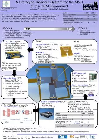
The Demonstrator Trb2 (TRBnet) demo-AUX analogue output Demonstrator project accomplished See talk of Samir sync. signals MAPS add-on board or monitoring data transfer: I/O-card data transfer: OP-link Beam test @ Cern-SPS Nov 2009 file server
Why a prototype? A prototype to meets the requirements for the CBM MVD • The project aims at improve: • low material budget • mechanical integration • cooling • fast sensor readout • scalable DAQ-system for the full MVD (e.g. 20 sensors first station) • a whole network structure • from the front-end to the PC s
Sensors of the prototype Current compromise Best values reached • Mimosa26 offers: • logic for data reduction • huge pixel array (form factor for the final MVD) • multiplexer for faster readout • inspiration for the final MVD sensor (MimoSIS-1) * best of M. Deveaux, ULISI kick-off meeting, GSI, Feb. 17-18, 2010
Mimosa26 analogue Outputs 9 hits/ row Mi26 protocol allows: ∑ 570 hits pixel array: 1152 columns x 576 rows (18,4 µm pitch and 115,2 µs readout time) chipslowcontrol correlated double sampling Signal discrimination Demonstrator: Mimosa20 with analogue readout 2.4Gbit/s uncompressed zerosuppressionlogic multiplexing Discri test Temp probe PLL JTAG Digital input Digital output Power 80 MHz 2 channels • ~ 80 Mbit/s (570 words of 16 bit • ~ 9120 bit/frame) 160 Mbit/s
The readout boards developed by IKF electronic workshop The Trbv2 (HADES) provides a flexible add-on board concept The add-on board with a FPGA Is mounted on the TRBv2 back side • high data-rate digital interface • connector (15 Gbit/s) • FPGA configuration • high data transfer with optical link • (2 Gbit/s) • application process interface (API) • power supply +5V,10A • clock distribution • readout board for 3x Mimosa 26 • platform to study online data specification for data reduction • compatibility with HADES DAQ (Trb2) for testing purposes
The prototype readout • A telescopetostudy: • Protocol • scalable (unique ID for 512 sensors) • time/triggerstamps (forassynchronousreadoutofthesensors) • safetyaspects (check- sumanddatalength) • datareduction (160 Mbit/s down to 80 Mbit/s) • bufferedreadout • JTAG chain • Online monitoring • Beam tests • Offline analysis/tracking (CBM-root) MAPS add-on Digi Aux PC I/O-card Mimosa26 controlchain 2m add-on + Trbv2 1x Start,clk,Rst (LVDS) 2m data output 133 Mbyte/s ~ 13 sensors 3x D0,D1,CLK (LVDS) PC JTAG 15 cm JTAG chain 3 stations „telescope“ 2m vacuum JTAG board
Scalable DAQ-system Digi Aux PC I/O-card Mimosa26 1x Start,clk,Rst (LVDS) add-on + Trbv2 • Tostudy: • Scalablesystem (unique ID forboards) • Board synchronisation • Repeaterforsignalconditioning MAPS add-on I/O limitation for only 3 sensors 3x D0,D1,CLK (LVDS) add-on + Trbv2 3x D0,D1,CLK (LVDS) MAPS add-on PC JTAG 1x RJ45 JTAG board
Data rate for the MVD Data rate of the sensors was simulated accounting for: pile-up, delta electrons, clustering, fake hits rates with the data protocols of Mimosa26 Conclusions: Total data rate of the MVD 10 GBytes/s Data rate of individual sensor < 2.4 Gbit/s Data reduction on FPGA boards First MVD station located at 5 cm See talk of S.Seddiki
New readout board 2m front-end 2x optical link (each 2 Gbit/s) >30 Mimosa26/board 3x LVDS clk/start/rst 4x LVDS JTAG 3x LVDS D0,D1,clk TRBv2 + add-on front-end digital chipdata via optical link (2 Gbit/s) N N S Algorithms have to be studied N N S front-end N N S - . . . • New add-on board: • chipcontrolling • chipmointoring • protocolfor front-ends • networkprotocol (TrbNet) • … (telescopestudies) MIMOSA26 readout: Seed pixel and the successive two Neighbor pixels • Trbv2: • JTAG • power supply • monitoring √ front-end The readoutboardcanbeusedascomputingnode • Fakehitsuppression clusterbuilding • Hit finding …
Hub-AddOn (HADES) • 20x up to 3.125 Gbit/s • (~1.2 Gbit/s raw data) • Capable of Gigabit-Ethernet to • send data to standard PCs (TCP) • Implements basic data processing • features • Buffered readout Successful tested
PC-Interface: PEXOR 3 • PCI-Express card (x4) • Fast Lattice SCM40 FPGA • 4 optical links up to 3.8 Gbit/s each • PCI-Express bus up to 4 Gbit/s Hardware available jet
MVD readout setup front-end front-end FPGA boards TrbNetprotocol See talk of B. Milanovic TRBv2 + addon TRBv2 + addon front-end front-end PC optical link- PCI-express-card upto 3.8 Gbit/s hub add-on +TRBv2 upto 2 Gbit/s front-end front-end . . . . . . PCI Express card 4x 3.8 Gbit/s PCI express bus: 4 Gbit/s ~ 50 x Mimosa26 unbuffered . . . Hub Input: 16 x optical links (8x 30 Mimosa26) Output: 4x optical links ~ 240 sensorsbuffered front-end front-end
The new front-end MIMOSA-26 Digi Aux • All in one • Highly integrated • Vacuum compatible • Suffix to cooling concept • Radiation tolerant • Bus concept • Advanced flex print cable (e.g. IMEC : sensors in ultra thin polyamide film) • … JTAG board
Thank you