Download
1 / 32
360 likes | 429 Vues
Explore fundamental topics in solar cell semiconductor physics, including wavelength, frequency, and energy of electromagnetic waves. Learn about the spectrum of solar and visible light, photon energy, irradiance, and semiconductor properties.

E N D
Basic Fundamentals of Solar Cell Semiconductor Physics
Wavelength and Frequency Period (sec) amplitude time Frequency (n) = 1/Period [cycles/sec or Hertz] Wavelength (l) = length of one Period [meters] For an electromagnetic wave c = nl,where c is the speed of light (2.998 x 10⁸ m/sec)
Spectrum Intensity Frequency (n) Range of frequency (or wavelength, c/n) responses or source emissions. The human eye has a response spectrum ranging from a wavelength of 0.4 microns (0.4 x 10⁻⁶ meters) (purple) to 0.8 microns (red)
Solar Spectrum at Earth Surface (noon time) 925 W/m2 E (eV) = hc/l l = hc/E Visable range .75 mm (red) - .4 mm (purple) 1.6 eV - 3.1 eV Solar Spectrum at Earth Surface .5 eV - 3.6 eV 2.6 mm (infrared) - 0.34 mm (ultraviolet) visible inrfared ultraviolet Solar Spectrum at Earth Surface (noon time)
Energy and Power Electromagnetic waves (light, x-rays, heat) transport energy. E = hn or hc/l [Joules or eV (electron-volts)] 1 eV = 1.6 x 10⁻¹⁹ Joules h = Plank’s constant (6.625 x 10⁻³⁴ Joule-sec or 4.135 x 10⁻¹⁵ eV-sec) n = frequency c = speed of light l = wavelength Power is the amount of energy delivered per unit time. P = E/t [Joules/sec or Watts]
Photons A light particle having energy. Sunlight is a spectrum of photons. X-rays and heat are photons also. Photon Energy E = hn or hc/l [Joules or eV (electron-volts)] (higher frequency = higher energy) (lower energy)
Irradiance Amount of power over a given area, Watts/m2 4 red photons every second Area = 2.00 m2 Energy of 1 red photon = hc/l = (6.63 x 10⁻³⁴ J-s)(2.99 x 10⁸ m/s)/(0.80 x 10-6 meters) = 2.48 x 10⁻¹⁹ J = 1.55 eV Irradiance = Power/Area = (4 photons/sec)(Energy of 1 photon)/2.00 m2 = 4.96 x 10⁻¹⁹ W/m2 Typical sunlight irradiance is 0.093 W/cm2 = 930 W/m2 at l = .55 mm
Transmission, Reflection, and Absorption incident light reflectance (R) air transmittance (T) + absoprtance (A) material • Incident light = T + R + A = 100% • Non-transparent materials have either very high • reflection or very high absorption. • Absorption decreases transmission intensity with • increasing depth into material.
Polarization Polarizer Unpolarized light (e.g. sunlight) Linearly polarized light Only one plane of vibration passes
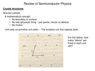
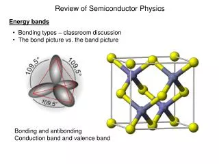
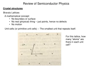
Semiconductor Crystal Lattice atom covalent bond Simple Cubic Structure Silicon has a more complex lattice structure but a lattice structure exists nevertheless.
Crystalline Silicon Bonds valance electrons Si atom (Group IV) = covalent bond (electron sharing)
+ Breaking of Covalent Bond Creating Electron-Hole Pair free electron moving through lattice e- created hole (missing electron) covalent bond Si atom Photon (light, heat) Photon hits valance electron with enough energy to create a free electron and hole
+ + Movement of a Hole in a Semiconductor Thermal energy causes a valance electron to jump to an existing hole leaving a hole behind
e- + Valance and Conduction Energy Bands free electron moving in lattice structure Conduction Energy Band Ec Band Gap Energy, Eg = Ec - Ev Valance Energy Band Ev Hole within valance band covalent bonds
Valance and Conduction Energy Bands Thermal Equilibrium e- e- + + free electron combines with hole free electron within lattice structure Conduction Energy Band Ec Eg Heat enery given up Heat energy absorbed Valance Energy Band Ev Hole created within valance band covalent bonds Energy absorbed = Energy given up
e- + Intrinsic (pure) Silicon Electron-Hole Pairs Thermal Equalibrium ni = 1.5 x 1010 cm-3 at 300° K Conduction Band Ec hole density = electron density number of holes per cubic centimeter = number of free electrons per cubic centimeter pi = ni = 1.5 x 1010 cm-3 Eg = 1.12 eV pi = 1.5 x 1010 cm-3 at 300° K Valance Band Ev covalent bonds • Number of electron-hole pairs increase with increasing temperature
Doping or Substitutional Impurities Group V Atom (Donor or N-type Doping) Phospherous (Group V) P atom e- covalent bond Si atom (Group IV) The donor electron is not part of a covalent bond so less energy is required to create a free electron
e- e- + Energy Band Diagram of Phospherous Doping intrinsic free electron donor free electron Conduction Band Ec Donor Electron Energy n > p (more electrons in conduction band) A small amount of thermal energy elevates the donor electron to the conduction band Eg Ev Valance Band intrinsic hole covalent bonds N-type Semiconductor
- + Doping or Substitutional Impurities Group III Atom (Acceptor or P-type Doping) Boron (Group III) B atom covalent bond created hole covalent bond Si atom Boron atom attacts a momentarily free valance electron creating a hole in the Valance Band
e- e- + + Energy Band Diagram of Boron Doping intrinsic free electron Conduction Band Ec p > n (more holes in valance band) A small amount of thermal energy elevates the acceptor electron to the Acceptor band Eg acceptor electron Acceptor Electron Energy Ev Valance Band created hole intrinsic hole covalent bonds P-type Semicondutor
Formation and Basic Physics of PN Junctions
PN Junction Formation Masking Barrier Boron Atom Doping Phophorous Atom Doping Intrinsic Silicon Wafer • Doping Atoms are accelerated towards Silicon Wafer • Doping Atoms are implanted into Silicon Wafer • Wafer is heated to provide necessary energy for Doping Atoms to become • part of Silicon lattice structure
PN Junction in Thermal Equilibrium (No Applied Electric Field) Space Charge Region metallurgical junction metallurgical junction - - - - + + + + P-type N-Type p n Initial Condition E field Equilibrium Condition • Free electrons from n-region migrate to p-region leaving donor atoms behind. • Holes from p-region migrate to n-region leaving acceptor atoms behind. • Internal Electric Field is created within Space Charge Region.
e- e- e- e- e- + + + + + PN Junction Solar Cell Operation Photon hn > Eg Space Charge Region E field p n • Photons create hole-electron pairs in space charge region • Created hole-electron pairs swepted out by internal E field • Excess holes in p-region • Excess electrons in n-region
e- e- e- e- e- + + + + + PN Junction Solar Cell Operation Photon hn > Eg Space Charge Region E field p n Icell Resistor - + Vcell • Attaching a resistive load with wires to the PN Junction creates • current flow from p to n regions • Electrons flow from n-region to combine with holes in p-region • Photons create new hole-electron pairs to replace combined pairs
Typical Silicon Solar Cell Design Photons Protective High Transmission Layer P-type Doping Wires N-type Silicon Wafer 0.6 mm 4-6 inches To load • Photons transmit through thin protective layer and • thin P-type doped layer and create hole-electron • pairs in space charge region • Typical Silicon Single Cell Voltage Output = ~ 0.5 volts
Silicon Solar Cell 6 Volt Panel Series-Parallel Design 12 cells in series = 6 volts p to n connection - 6 volts +
External Factors Influencing Solar Cell Effeciency • Photon transmission, reflection, and absorption of protective layer • Maximum transmission desired • Minimum reflection and absorption desired • Polarization of protective layer • Minimum polarized transmission desired • Photon Intensity • Increased intensity (more photons) increases cell current, Icell • Cell voltage, Vcell, increases only slightly • Larger cell area produces larger current (more incident photons) • Theoretical Silicon Solar Cell Maximum Efficiency = 28% • Typical Silicon Solar Cell Efficiency = 10-15%