Optical Properties at the Nanoscale
830 likes | 1.52k Vues
Optical Properties at the Nanoscale. James L. Merz Department of Electrical Engineering Department of Physics University of Notre Dame EE 698D – Advanced Semiconductor Physics Notre Dame 23 November 2004. References. ► Primary reference for this talk:

Optical Properties at the Nanoscale
E N D
Presentation Transcript
Optical Properties at the Nanoscale James L. Merz Department of Electrical Engineering Department of Physics University of Notre Dame EE 698D – Advanced Semiconductor Physics Notre Dame 23 November 2004
References ► Primary reference for this talk: Quantum Semiconductor Structures, Fundamentals and Applications, C. Weisbuch and B. Vinter, Academic Press, Inc., San Diego, 1991. (referred to throughout the talk as W & V.) ► The Quantum Dot, R. Turton, Oxford Univ. Press, NY, 1995. ► Quantum Dot Heterostructures, D. Bimberg, M. Grundmann, and N.N. Ledentsov, John Wiley and Sons, Chichester, England, 1999 ► Electronic and Optoelectronic Properties of Semiconductor Structures, J. Singh, Cambridge Univ. Press, Cambridge, 2003.
References (continued) ► Many of the slides were taken from a Plenary talk by Maurice Skolnick at the International Conference on the Physics of Semiconductors (ICPS), Flagstaff, AZ (July 2004). Used with his permission. ►"Near-field Magneto-photoluminescence Spectroscopy of Composition Fluctuations in InGaAsN", A.M. Mintairov, J.L. Merz, et al, Phys. Rev. Letters 87, 277401 (31 December 2001); “Exciton Localization in InGaAsN and GaAsSbN Observed by Near-field Magnetoluminescence”, James L. Merz, A.M. Mintairov et al, Proceedings of the Spring meeting of the European Marterials Research Society, Symposium M, to be published in IEE Proceedings Optoelectronics.(referred to in the talk as M & M)
How do we make Quantum Wells (QWs)? ► Typically by MBE or MOCVD. ► Grow thin films (a few monolayers to tens of monolayers) of a narrow-bandgap semiconductor bounded by a wider-bandgap semiconductor. ► The process can be repeated several times or many times, to make multiple (non-interacting) QWs, or a superlattice of interacting QWs.
Fundamentals of Quantum-Confined StructuresQuantum Wells (1-D structures) W & V, pg. 3, Fig.1
“Classical” Quantum Mechanical Problem: Particle in a Box ►These structures are best grown by Molecular Beam Epitaxy (MBE) or Metal-Organic Chemical Vapor Deposition (MOCVD) ► Let the potential barriers be infinitely high ► Solve the Schrödinger Equation for this one-dimensional case ► Solutions are sinusoidal functions: Ψ(z) = sin(kz) or cos(kz), where z is growth direction. ►Solutions must vanish at the well/barrier interfaces (i.e., Ψ(z)= 0 at z = 0 and z = b, where b is the thickness of the film)
Eigenfunctions and Eigenvalues W & V, pg. 12, Fig. 5
Finite barrier (Vo) allows exponential penetration into the barrier W & V, pg. 13, Fig.6 Note that this problem is mathematically equivalent to the dielectric waveguide. Energy eigenstates then become guided optical modes.
Coupled Quantum Wells W&V, pg. 29, Fig.14 ► As two wells approach each other, their wave functions overlap ► This leads to a pair of eigenstates which split into two levels ► For many coupled wells, get multiple states → energy band
Superlattice Energy Bands ►At a given well or barrier width a, the higher energy states become broader bands. This results from the fact that the wave function overlap increases for the higher-lying energy eigenstates. ►Thus, for a = 50 Å, E1 is a discrete state, while E2, E3,E4, etc. form successively broader bands. W & V, pg. 38, Fig.18c
AlxGa1-xAs:an ideal material to form Quantum Wells and Superlattices Energy Gap Eg (eV) ► For 0 < x < 0.4 AlxGa1-xAs has a direct bandgap that is larger than GaAs. ► GaAs and AlGaAs are very nearly lattice matched. ► Thus, AlGaAs is an excellent potential barrier for GaAs quantum wells. H.C. Casey and M.B. Panish, J. Appl. Phys. 40, 4910 (1969).
Optical absorption of multiple uncoupled quantum wells – comparison with bulk GaAs: Eg= 1.43 eV Al.3Ga.7As: Eg = 1.79 eV 50 periods of 100 Å GaAs = .5 mm Comparison with 1 mm bulk GaAs W & V, pg. 64, Fig.30e
What are the differences?? ► For quantum wells, the absorption edge is at higher energy than the bulk absorption edge, due to increased energy of the confined state in the GaAs quantum well. ► Bulk GaAs shows √E energy dependence due to direct gap of GaAs (3-D bulk density of states). ► GaAs quantum well absorption shows “stair case” dependence on energy (2-D density of states). ► Sharp peaks are due to exciton absorption. ► Some corrections must be made for e-h correlation effects.
What is the Density of States? ► The density of states is the number of states per unit volume per unit energy interval that are available for occupation by electrons (or holes). ► Optical absorption must be proportional to the density of states, because a photon cannot be absorbed if there is no final state available for the electronic transition. ► For 3-D parabolic bands (bulk), ICBSTN(E)= (1/2p2)(2m*/ħ2)3/2√E, where m* is the effective mass of the electron. ► For a 2-D quantum well, ICBST N(E)= m*/pħ2, independent of E. For each quantum state in the quantum well, there will be a step in the density of states.
Absorption of Bulk Semiconductors:Direct and Indirect Bandgap ►Direct Bandgap: a ~ (hn – Eg)1/2 ► Indirect Bandgap: Must have momentum conservation Absorb a phonon: aa ~ (hn – Eg + ħw)2 Emit a phonon: ae ~ (hn – Eg – ħw)2
2-D and 3-D Density of States W & V, pg. 21, Fig.10
Excitons ► Exciton: photon produces electron-hole pair. ►Electron-hole pair is bound by Coulomb attraction, losing energy and creating sharp energy states (analogous to H2 atom) ► The 2-D Rydberg is 4x greater than the 3-D Rydberg. ► Sommerfeld factor is due to electron-hole correlation in unbound states. W & V, pg.26, Fig.13
Excitons and Shallow Impurities ► Hydrogen atom: e2/err term gives series of energy states: En = ERydb/n2, where ERydb = e4mo/2ħ2 = 13.6 eV, and the Bohr radius aB = ħ2/moe2 = 0.529 Å. ► For a donor, must correct for the electron mass and the dielectric constant: En = (me*/er2)ERydb → 10-20 meV ► For an exciton, must use reduced mass: 1/m = 1/me* + 1/mh* En = (mr*/er2)ERydb → 5-20 meV
The 2-D Rydberg ► Can solve the problem for an infinite potential model ERydb2-D = ERydb3-D * 1/(n – ½)2 = ERydb3-D * 4/(2n-1)2 Ground state: n = 1 → ERydb2-D = 4 * ERydb3-D
Optical absorption of multiple uncoupled quantum wells – comparison with bulk GaAs: Eg= 1.43 eV Al.3Ga.7As: Eg = 1.79 eV 50 periods of 100 Å GaAs = .5 mm Comparison with 1 mm bulk GaAs W & V, pg. 64, Fig.30e
Dependence of exciton binding energy (EBX)on quantum well thickness ► For an infinite well, EBX increases as the well gets thinner, just as does the single-electron state. ► For a finite well, EBX reaches a max. and then decreases because e and h wave functions spread out into the barrier. ► As d becomes very large, the light hole binding energy > heavy hole because EBX ~ 1/mass. ----- Light-hole exciton _____ Heavy-hole exciton W & V, pg. 25, Fig.12
Optical Absorption of Coupled Wells ► (a) Single well: one state, split into heavy & light hole. ► (b) Double well: two states (bonding and antibonding), each of which is split into heavy & light hole. ► (c) Triple well: three states, each split into heavy & light hole. W & V, pg.73,Fig.35 Dingle et al, Phys.Rev.Lett. 34, 1327 (1975) Dingle et al, Phys.Rev.Lett. 33, 827 (1974)
Effect of Quantum Well Thickness ► In layer-to-layer growth mode, one expects thickness variations of ~0.5 monolayer from average monolayer thickness. ► Intralayer thickness fluctuations cause variations of confining energies. ► For thin wells (51Å), these variations cause a larger relative effect, hence lines broaden. ► Note increase in photon energy of absorption edge as well gets thinner, as expected. W & V, pg.76, Fig.38
Franz-Keldysh Effect for Bulk Material ► Bulk material Applied field E ≠ 0 Franz-Keldysh Effect: bands are tilted. ► Absorption below Eg because of exponential wave-function tails. ► Oscillations above Eg due to wave-function interference. W & V, pg.89, Fig.46
Quantum-Confined Stark Effect (QCSE) ► Quantum Well, E = 0 Usual case seen before. ► Quantum Well, E ≠ 0 Bands tilt and energy of quantum states decreases → “red” shift of luminescence energy. Wave function overlap decreases → reduction of luminescence intensity. W & V, pg.89, Fig.46
Optical Absorption due to QCSE ► Values of applied electric field: (i) E = 0 (ii) E = 60 kV/cm (iii) E = 110 kV/cm (iv) E = 150 kV/cm (v) E = 200 kV/cm ► The predicted red shift and intensity decrease are both observed with increasing electric field. W & V, pg.90, Fig.47
Wannier-Stark Localization (WSL) ► QCSE is observed for a single QW. ► WSL is observed for a QW superlattice. ► At E = 0 the discrete QW states form bands in a superlattice, and the electron can be anywhere in the superlattice. ► As E increases, the superlattice bands tilt, and the energy eigenstates no longer overlap. Bands get narrower and then coalesce into sharp states. ► At high electric fields, the electron is completely localized. Mendez et al, Phys.Rev.Lett. 60, 2426 (1988)
Formation of “Stark Ladders” in WSL QCSE red shift At low E-field, e is delocalized. With increasing E, up to 5 states are seen, which reduce to one at high field. Plot of photocurrent peak energies vs. E. Stark ladders from outlying states are clearly seen, which quickly disappear at high field. Mendez et al, Phys.Rev.Lett. 60, 2426 (1988)
n-i-p-i Structures ► These are n-i-p-i homojunctions. ► Electrons from n region fall into holes in p regions, leaving ionized impurities. ► Resulting space charge distribution modulates the bands, forming energy eigenstates. ► The result is a homojunction superlattice. W & V, pg.52, Fig.27
n-i-p-i Light Modulation Phenomena Turton, pg.134, Fig.8.8 In the dark, the n-i-p-i structure has reduced the effective bandgap of the structure, as shown by the energy arrow in (a). If above-bandgap monochromatic light is incident on the structure, electrons and holes are produced which reduce the space charge, flattening the bands and increasing the radiative recombination energy, as shown by the energy arrow in (b). Thus, changes in the intensity of monochromatic light shining on the sample changes the wavelength of the emission.
Semiconductor Lasers ► electrons and holes are injected into GaAs active region by p-n junction. ► Carriers are confined to active region by potential barriers. ► Photons are confined to active region by refractive index difference. W & V, pg.166, Fig.88
Confinement of Optical Guided Wave ► Double Heterostructure – Optical mode well confined. Too many electron states available. G ~ 1 ► Single Quantum Well Optical mode poorly confined. Electrons well confined to single state. G ~Dn d2 ► Separate Confinement Heterostructure Optical mode moderately confined to the quantum well. Electrons well confined. G ~ Dn d W& V, pg.168, Fig.89
Confinement Factor (G) d/2 ∞ G = ∫│E (z)│2dz /∫│E (z)│2dz -d/2-∞
Threshold Current Density (Ith) W & V, pg.171, Fig.92 ►Want to minimize Ith. ►GSCH is Graded-index Separate Confinement Heterostructure (also called GRINSCH)
Vertical Cavity Surface Emitting Laser (VCSEL) ► Active layer: GaInAs/GaAs QWs ► Mirrors: GaAs/AlGaAs multiple layers with thickness ~ optical wavelengths → Distributed Bragg Reflectors (DBRs) ► Advantages: • Low Ith due to QW active layer (Ith≤400 A/cm2) • Very low I (<70 mA) due to small cross-sectional area (8 mm) • Low output diffraction → can couple efficiently into optical fibers • Can make large arrays Huffaker & Deppe, Appl. Phys. Letters 70, 1781 (1997). W & V, pg.183, Fig.102a
VCSEL Arrays J. Jewell et al, Appl. Phys. Letters 55, 2724 (1989)
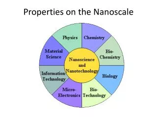
Thus far: ►We solved the Schrödinger Equation for the one-dimensional “particle in a box” ► These results were appropriate for a two-dimensional semiconductor structure i.e., a quantum well ► Now we are interested in confinement in two and three directions, leading to structures that are one-dimensional and zero-dimensional, respectively i.e., quantum wires and quantum dots or boxes. ► We also said that we could derive the so-called “density of states”, and that this concept is very important to understand electrical and optical phenomena of these quantum-confined structures. ►Now the concept of density of states becomes increasingly important, and for quantum wires and dots the experimental techniques of single-electron transport (Snider) and near-field optics (Merz) become increasingly important.
2-D and 3-D Density of States W & V, pg. 21, Fig.10
Early Prediction about Quantum Wires ► Hiroyuki Sakaki1 predicted, more than two decades ago, that ideal 1-D electrons moving at the Fermi level in quantum wires would require very large momentum changes (Dk = 2kF, where kF is the Fermi wave-vector) to undergo any scattering, ► The result would be that electron scattering would be strongly forbidden. ► This is a consequence of the fact that in one dimension, electrons can scatter only in one of two directions: forward and 180o backwards. ► With this large reduction in scattering, electrons would achieve excellent transport properties (e.g., very high mobility). 1 H. Sakaki, J. Vac. Sci. Technol. 19(2), 148 (1981)
Early Prediction about Quantum Dots ► A year later, Arakawa and Sakaki1 predicted significant increases in the gain, and decreases in the threshold current, of semiconductor lasers utilizing quantum dots or boxes in the active layer of the laser. ► Highly efficient, low power lasers could be the consequence of these predictions. ► These predictions set off an intense effort worldwide to fabricate such structures. 1 Arakawa and Sakaki, Appl. Phys. Letters 40, 939 (1982)
Low-dimensional Semiconductor LaserPerformance Calculations Asada, Miyamoto, & Suematsu, IEEE J. Quantum Electronics QE-22, 1915 (1986)
Why are Quantum Dots Important • SAQDs important for both physics and applications • Strong confinement and high radiative efficiency • Quasi-0D systems in the solid state. ‘Atom-like’ • Embedded in semiconductor matrix. Wide variety of semiconductor devices, processing technology from Skolnick
well bulk 3D 2D Density of States 1D 0D dot wire Energy (a) (b) 0 (c) (d) 0 Modification of Density of States by Reduction of Dimensionality from Skolnick
General approaches to QD synthesis Colloidal growth of CdSe dots Artificial patterning Self-assembled quantum dots (SAQDs) by MBE Bimberg et al, pg.5, Fig.1.3
Colloidal CdSe QDs Colloids of CdSe QDs are fluorescent at various frequencies within the visible range. The highly tunable nature of the QD size yields a broad range of colors in the visible spectrum. E. Karreich, Nature 413, 450 (2001)
Self-Assembled Crystal Growth of QDs in Strained Systems by MBE Stranski-Krastanow growth InAs-GaAs 7% lattice mismatch Note wetting layer Most important system: InAs GaAs Embedded in crystal matrix – like any other semiconductor laser or light emitting diode from Skolnick
QDs WL Quantum Dots and the Wetting layer UHV-STM cross sections PM Koenraad, TU Eindhoven 20nm from Skolnick