Dielectric isolation
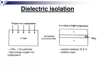
Dielectric isolation. annealing. - <100> n Si substrate - high energy oxygen ion implantation. - reaction between Si & O - isolation layer. SiO 2. - etching a trench and refilling with oxide. - Creating of n-p-n structure. - high breakdown voltage C-E (several hundreds volts).

Dielectric isolation
E N D
Presentation Transcript
Dielectric isolation annealing - <100> n Si substrate - high energy oxygen ion implantation - reaction between Si & O - isolation layer
SiO2 - etching a trench and refilling with oxide - Creating of n-p-n structure - high breakdown voltage C-E (several hundreds volts)
Polysilicon bipolar structure • n type epitaxial layer • p substrate • etchingthrough n to p area • polysilicon layer deposition • heavy boron doping • CVD of O a N • dry etching throuhg vaporized layers
oxide is grown on vertical sidewalls of • doped poly • p+ extrinstic regions are formed • in substrate • ion implantaion of boron to create • intrinstic base area • -second polysilicon layer – As,P implant
- Pt film is deposited and sintered to create PtSi over the emmiter and base contacts