2.11 VOLTAGE-MULTIPLIER CIRCUITS
330 likes | 901 Vues
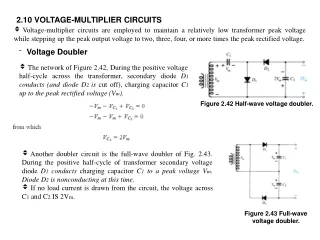
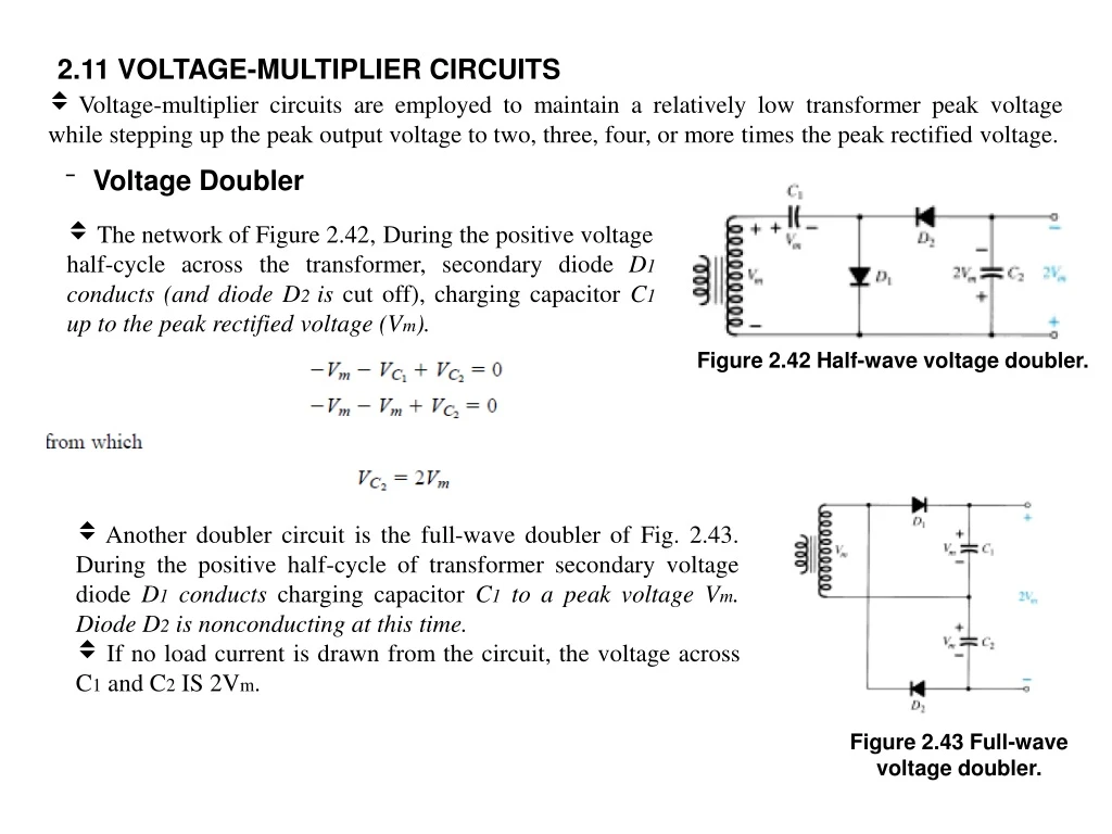
2.11 VOLTAGE-MULTIPLIER CIRCUITS. Voltage-multiplier circuits are employed to maintain a relatively low transformer peak voltage while stepping up the peak output voltage to two, three, four, or more times the peak rectified voltage. Voltage Doubler.

2.11 VOLTAGE-MULTIPLIER CIRCUITS
E N D
Presentation Transcript
2.11 VOLTAGE-MULTIPLIER CIRCUITS • Voltage-multiplier circuits are employed to maintain a relatively low transformer peak voltage while stepping up the peak output voltage to two, three, four, or more times the peak rectified voltage. • Voltage Doubler • The network of Figure 2.42,During the positive voltage half-cycle across the transformer, secondary diode D1 conducts (and diode D2 is cut off), charging capacitor C1 up to the peak rectified voltage (Vm). Figure 2.42 Half-wave voltage doubler. • Another doubler circuit is the full-wave doubler of Fig. 2.43. During the positive half-cycle of transformer secondary voltage diode D1 conducts charging capacitor C1 to a peak voltage Vm. Diode D2 is nonconducting at this time. • If no load current is drawn from the circuit, the voltage across C1 and C2 IS 2Vm. Figure 2.43 Full-wave voltage doubler.
Voltage Tripler and Quadrupler • Figure 2.44 shows an extension of the half-wave voltage doubler, which develops three and four times the peak input voltage. In operation capacitor C1 charges through diode D1 to a peak voltage, Vm, during the positive half-cycle of the transformer secondary voltage. Capacitor C2 charges to twice the peak voltage 2Vm developed by the sum of Figure 2.44 Voltage tripler and quadruple the voltages across capacitor C1 and the transformer, during the negative half-cycle of the transformer secondary voltage. • During the positive half-cycle, diode D3 conducts and the voltage across capacitor C2 charges capacitor C3 to the same 2Vm peak voltage. On the negative halfcycle, diodes D2 and D4 conduct with capacitor C3, charging C4 to 2Vm. • The voltage across capacitor C2 is 2Vm, across C1 and C3 it is 3Vm, and across C2 and C4 it is 4Vm. If additional sections of diode and capacitor are used, each capacitor will be charged to 2Vm. Measuring from the top of the transformer winding (Fig.2.44) will provide odd multiples of Vm at the output, whereas measuring the output voltage from the bottom of the transformer will provide even multiples of the peak voltage, Vm.
2.12 power supply • Introduction: • Starting with an ac voltage, we abtain asteady dc voltage by rectifying the ac voltage, then filtering to a dc level and finally, regulating to obtain a desired fixed dc voltage . A block diagram containing the parts of atypical power supply is shown in fig.(2. 45). Fig.(2. 45) Block diagram showing parts of power supply.
When the diode is in it’s short- circuit state the output voltage will be directly across the 4-V dc supply. Requiring that the output be fixed at 4V. In other words, when the diode is on the output will be 4V, other than that, when the diode is an open circuit, the current through the series network will be 0mA and the voltage drop across thr resistor will be 0V. That will result in VO ≈ Vi whenever the diode is OFF. Step-3. The transition level of the input voltage can be found from Fig. 2.29, by substituting the short – circuit equivalent and remembering the diode current Id = 0 mA at the instant of transition. The result is a change in state when Vi = 4 V. Step-4. The transition level is drawn along with Vo = 4V when the diode is on. For Vi ≥4V. Vo = Vi . • If we repeat the Example using a silicon diode with VK = 0.7V. Solution: The transition voltage can be first be determined by applying the condition Id= 0A at Vd =VD = 0.7V and obtaining the network of Fig. (2. 30). Applying KVL around the output loop in the clockwise direction, we find that : Vi + VK – V = 0 Vi = V - VK = 4V – 0.7 = 3.3V with Vi ˃ 3.3 V, the diode open and VO = Vi . For Vi ˂ 3.3V, the diode “on” state VO = 4V – 0.7 = 3.3V Figure 2.30 Determining the transition level for the network of Fig. 2.28. Figure 2.31