Download
1 / 7
80 likes | 179 Vues
This presentation discusses an adjustable transconductance amplifier with noise compensation, detailing the overall topology, basic operational principles, variable gain amplifier features, theoretical and actual linear range, stability, circuit details, and noise impact considerations.

E N D
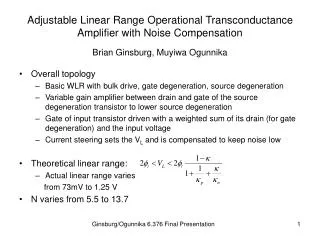
Adjustable Linear Range Operational Transconductance Amplifier with Noise Compensation Brian Ginsburg, Muyiwa Ogunnika • Overall topology • Basic WLR with bulk drive, gate degeneration, source degeneration • Variable gain amplifier between drain and gate of the source degeneration transistor to lower source degeneration • Gate of input transistor driven with a weighted sum of its drain (for gate degeneration) and the input voltage • Current steering sets the VL and is compensated to keep noise low • Theoretical linear range: • Actual linear range varies from 73mV to 1.25 V • N varies from 5.5 to 13.7 Ginsburg/Ogunnika 6.376 Final Presentation
gs -A/gmp gmp + Vin gmb + iout gm 1/gmn 1-A A + Block Diagram 0<A<1 Ginsburg/Ogunnika 6.376 Final Presentation
Variable Linear Range Performance • Linear range varies from 73mV to 1.248V • Each OTA has 45 transistors • Common mode input range is from 1.25V to 3 V at highest current levels; increases to 0.85V-3V at low bias current levels • In resonant filter, f90 can vary from 100Hz to 10kHz, and Q can be variable from 1 to 6, though not for all VL Ginsburg/Ogunnika 6.376 Final Presentation
Stability of the OTA • No load capacitor • 1kHz bandwidth • 100mV linear range • Unity-gain feedback • <5% overshoot in step response • OTA also stable with 10% component mismatch • Power with 5pF cap and 10kHz bandwidth <3.47μW Ginsburg/Ogunnika 6.376 Final Presentation
IHVLkg ILVLkg ILVLks ILVLks 2IBSks Circuit Details Gate Drive Weighted Adder Variable Gain Amplifier Ginsburg/Ogunnika 6.376 Final Presentation
Noise Impact of VL Variation Effective number of noise sources from gate drive circuit: Theoretical N vs. VL • Observations • For fixed VL, as IB drops, noise improves for fixed IBS • As VL decreases, noise shoots up • Solutions • For fixed VL, have IBS=kbIB • Make kb inversely dependent on VL • IBS=(1+6(1-A))IB/20 • Power overhead varies from 30% to 130% Dashed: Fixed kb Solid: Variable kb Actual N vs. VL • At Q=2, 10kHz • VL=1.25, N=5.4 • 21.3μW • 0.4dB variation from unity in passband, >50dB attenuation at high frequencies Ginsburg/Ogunnika 6.376 Final Presentation
Final Layout • Fits in less than one quarter of the chip! • Most of the additional circuitry is kept very small • Conclusions • Questions Ginsburg/Ogunnika 6.376 Final Presentation