Download
1 / 23
250 likes | 1.44k Vues
Learn the fundamentals of series and parallel AC networks, including impedance visualization, applying KVL and KCL, and VDR/CDR applications. Explore resistive, inductive, and capacitive reactance with phasor diagrams and waveform examples.

E N D
RLC Series and Parallel Circuit Department of Electrical Engineering BY:- Shah Krishnaji Patel Daxil Patel Dakshit Patil Parita S. Panchal Swapnil Guided by:-Prof. (Dr.) A. R. Chudasama Mrs. Nidhi Gohil Neotech Institute of Technology
OBJECTIVES • Become familiar with the characteristics of series and parallel ac networks and be able to find current, voltage, and power for each element. • Be able to find the total impedance of any series or parallel ac network and sketch the impedance and admittance diagram of each. • Applying KVL and KCL to any series or parallel configuration. • Be able to apply the VDR or CDR to any ac network. Neotech Institute of Technology
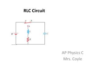
FIG. 15.1 Resistive ac circuit. IMPEDANCE AND THE PHASOR DIAGRAMResistive Elements • For purely resistive circuit v and i were in phase, and the magnitude: • In phasor form, Neotech Institute of Technology
FIG. 15.5 Waveforms for Example 15.2. FIG. 15.4 Example 15.2. IMPEDANCE AND THE PHASOR DIAGRAMResistive Elements Neotech Institute of Technology
FIG. 15.9 Waveforms for Example 15.3. FIG. 15.8 Example 15.3. IMPEDANCE AND THE PHASOR DIAGRAMInductive Reactance • for the pure inductor, the voltage leads the current by 90° and that the reactance of the coil XLis determined by ψL. Neotech Institute of Technology
FIG. 15.12 Phasor diagrams for Examples 15.3 and 15.4. IMPEDANCE AND THE PHASOR DIAGRAMInductive Reactance Neotech Institute of Technology
FIG. 15.17 Waveforms for Example 15.6. FIG. 15.16 Example 15.6. IMPEDANCE AND THE PHASOR DIAGRAMCapacitive Reactance • for the pure capacitor, the current leads the voltage by 90° and that the reactance of the capacitor XCis determined by 1/ψC. Neotech Institute of Technology
FIG. 15.18 Phasor diagrams for Examples 15.5 and 15.6. IMPEDANCE AND THE PHASOR DIAGRAMCapacitive Reactance Neotech Institute of Technology
FIG. 15.19 Impedance diagram. IMPEDANCE AND THE PHASOR DIAGRAMImpedance Diagram • Now that an angle is associated with resistance R, inductive reactance XL, and capacitive reactance XC, each can be placed on a complex plane diagram. Neotech Institute of Technology
FIG. 15.20 Series impedances. SERIES CONFIGURATION Neotech Institute of Technology
FIG. 15.41 Example 15.10. VOLTAGE DIVIDER RULE Neotech Institute of Technology
FIG. 15.46 Reviewing the frequency response of the basic elements. FREQUENCY RESPONSE FOR SERIES ac CIRCUITS Neotech Institute of Technology
ADMITTANCE AND SUSCEPTANCE • In ac circuits, we define admittance (Y) as being equal to 1/Z. • The unit of measure for admittance as defined by the SI system is siemens, which has the symbol S. • Admittance is a measure of how well an ac circuit will admit, or allow, current to flow in the circuit. • The larger its value, therefore, the heavier is the current flow for the same applied potential. • The total admittance of a circuit can also be found by finding the sum of the parallel admittances. Neotech Institute of Technology
FIG. 15.58 Parallel ac network. ADMITTANCE AND SUSCEPTANCE Neotech Institute of Technology
FIG. 15.59 Admittance diagram. ADMITTANCE AND SUSCEPTANCE Neotech Institute of Technology
FIG. 15.63 Example 15.14. FIG. 15.64 Impedance diagram for the network in Fig. 15.63. FIG. 15.65 Admittance diagram for the network in Fig. 15.63. ADMITTANCE AND SUSCEPTANCE Neotech Institute of Technology
FIG. 15.67 Parallel ac network. PARALLEL ac NETWORKS Neotech Institute of Technology
FIG. 15.77 Parallel R-L-C ac network. PARALLEL ac NETWORKSR-L-C Neotech Institute of Technology
FIG. 15.78 Applying phasor notation to the network in Fig. 15.77. PARALLEL ac NETWORKSR-L-C Neotech Institute of Technology
FIG. 15.79 Admittance diagram for the parallel R-L-C network in Fig. 15.77. FIG. 15.80 Phasor diagram for the parallel R-L-C network in Fig. 15.77. PARALLEL ac NETWORKSR-L-C Neotech Institute of Technology
FIG. 15.81 Waveforms for the parallel R-L-C network in Fig. 15.77. PARALLEL ac NETWORKSR-L-C Neotech Institute of Technology
FIG. 15.84 Example 15.17. FIG. 15.83 Example 15.16. FIG. 15.82 Applying the current divider rule. CURRENT DIVIDER RULE Neotech Institute of Technology
Thank you Neotech Institute of Technology
![[Series Circuit]](https://cdn1.slideserve.com/2747272/series-circuit-dt.jpg)