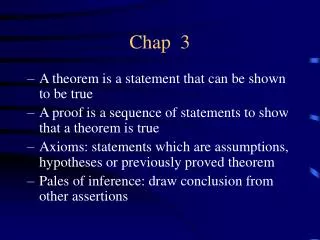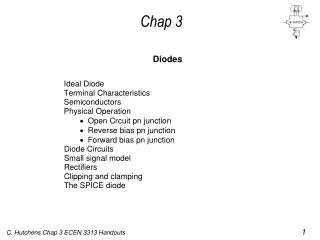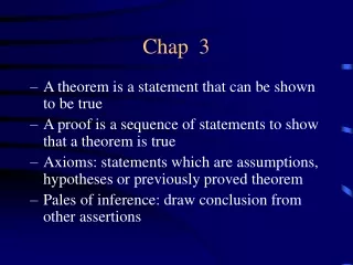
Chap. 3 Diodes
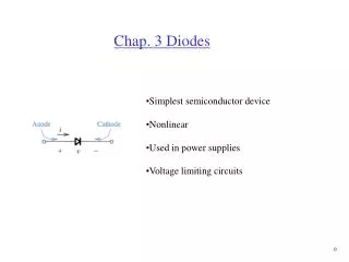
Chap. 3 Diodes. Simplest semiconductor device Nonlinear Used in power supplies Voltage limiting circuits. 3.1 Ideal Diodes. Reverse bias (off). Forward bias (on). I-V characteristics of an ideal diode. on. off. on. off. Ideal diode operation. Ideal diode operation. diode on

Chap. 3 Diodes
E N D
Presentation Transcript
Chap. 3 Diodes • Simplest semiconductor device • Nonlinear • Used in power supplies • Voltage limiting circuits
3.1 Ideal Diodes Reverse bias (off) Forward bias (on)
on off on off Ideal diode operation
Ideal diode operation diode on diode off
Ideal diode operation Vin =24 sinwt 24 12 Vout on off on off 30 Diode conducts when 24 sinwt = 12 sinwt = 12/24 wt = 30
Exercise 3.4(a) I + V - 2.5KW 5V Find I and V Assume diode is on. V= 0, I= 5V/ 2.5KW I= 2mA, implies diode is on. Correct assumption I 2.5KW 5V
Exercise 3.4(b) I + V - 2.5KW 5V Find I and V Assume diode is off. VD = - 5, ID = 0 implies diode is off. Correct assumption V= 5, ID = 0 2.5KW 5V
Exercise 3.4(e) Find I and V +3 (Start with largest voltage) Assume D1 on, then D2 will be off, and D3 will be off V = 3V, and I = 3V/1KW = 3mA. Check assumption, VD1 = 0, on VD2 = -1, off VD3 = -2, off Correct assumption (old-style OR gate) +2 +1 + V - I
3.6 Zener diodes • Designed to break down at a specific voltage • Used in power supplies and voltage regulators • When a large reverse voltage is reached, the diode conducts. • Vz is called the breakdown, or Zener voltage.
Typical use of Zener diode • The Zener diode will not usually conduct, it needs Vs > 12.5V to break down • Assume Vs fluctuates or is noisy • If Vs exceeds 12.5V, the diode will conduct, protecting the load
Solving ideal diode problems(determining if the diode is on or off) • Assume diodes are on or off. • Perform circuit analysis, find I & V of each diode. • Compare I & V of each diode with assumption. • Repeat until assumption is true.
Prob. 3.9(b) Are the diodes on or off? Assume both diodes are on. 10V = (10K)I1 I1 =10V/10K = I1 = 1mA 0 = (5K)I2 - 10V, I2 = 2mA Current in D2 = I2 = 2mA, on Current in D1 = I1 - I2 = -1mA, off Does not match assumption; start over. I1 I2
Prob. 3.9(b) Are the diodes on or off? I Assume D1 off and D2 on. 10V = (10K)I + (5K)I-10V 20V = (15K)I I = 20V/15K = 1.33mA Current in D2 = I = 1.33mA, on Voltage across D1 10V - 10K(1.33mA) = -3.33V, off Matches assumption; done.
Solving ideal diode problems(determining if the diode is on or off) • Assume diodes are on or off. • Perform circuit analysis, find I & V of each diode. • Compare I & V of each diode with assumption. • Repeat until assumption is true.
Prob. 3.10(b) Is the diode on or off? Assume diode on. 15V = (10K)I1 +(10K)(I1-I2) 15 = (20K)I1 -(10K)I2 1 0 = (10K)(I2-I1) +(10K)(I2-I3) 0 = -(10K)I1 +(20K)I2 -(10K)I3 2 0 = (10K)( I3-I2)+(10K)I3 + 10 -10 = -(10K)I2 + (20K)I3 3 I3 I1 I2 Put 3 into 2.-5 = -(10K)I1 +(15K)I2,Put 1 into this equation, solve for I2. I2 = 0.875mA, Current through diode is negative! Diode can’t be on.
Prob. 3.10(b) Assume diode off. 15V = (10K)I1 +(10K)I1 I1 = 0.75mA I2 = 0 0 = (10K)I3 +(10K)I3 + 10 I3 = -0.5mA V1 V2 I3 I1 I2 Find V1. V1 = (10K)I1 = 7.5V Find V2. V2 = -(10K)I3 = 5V Voltage across diode is V2 - V1 = -2.5V, diode is off
3.2 Real diodes Characteristics of a real diode breakdown Reverse bias Forward bias
Reverse bias region • A small current flows when the diode is • reversed bias, IS • IS is called the saturation or leakage current • IS 1nA • -VZ is the reverse voltage at which the diode • breaks down. • VZ is the Zener voltage in a Zener diode • (controlled breakdown). • Otherwise, VZ is the peak inverse voltage (PIV) IS
Forward bias region • For Silicon diodes, very little current • flows until V 0.5V • At V 0.7V, the diode characteristics are • nearly vertical • In the vicinity of V 0.7V, a wide range of • current may flow. • The forward voltage drop of a diode is often • assumed to be V = 0.7V • Diodes made of different materials have different voltage drops V 0.2V - 2.4V • Almost all diodes are made of Silicon, LEDs are not and have V 1.4V - 2.4V
3.4 Analysis of diode circuits(Simplified diode models) p. 159-162 • Ideal diode • Constant-voltage drop model • Constant-voltage drop model with resistor • All use assumptions because actual diode characteristics • are too difficult to use in circuit analysis
Constant-voltage drop model I-V characteristics • A straight line is used to represent the fast-rising characteristics. • Resistance of diode when slope is vertical is zero.
Constant-voltage drop model I-V characteristics and equivalent circuit + 0.7V - 0.7V
Constant-voltage drop with resistor model I-V characteristics • A straight line with a slope is used to represent the fast-rising characteristics. • Resistance of diode is 1/slope.
Constant-voltage drop with resistor model I-V characteristics and equivalent circuit + 0.7V 50W - 0.7V
Prob. 3.9(b) (using constant voltage-drop model) Are the diodes on or off? Assume both diodes are on. 10V = (10K)I1 + 0.7 I1 =9.3V/10K = I1 = 0.93mA 0 = -0.7 + 0.7 + (5K)I2 - 10V, I2 = 2mA Current in D2 = I2 = 2mA, on Current in D1 = I1 - I2 = -1.07mA, off Does not match assumption; start over. I1 I2
Prob. 3.9(b) (using constant voltage-drop model) Are the diodes on or off? I Assume D1 off and D2 on. 10V = (10K)I + 0.7 + (5K)I-10V 19.3V = (15K)I I = 19.3V/15K = 1.29mA Current in D2 = I = 1.29mA, on Voltage across D1 10V - 10K(1.29mA) = -2.9V, off Matches assumption; done.
Prob. 3.10(b) (using constant voltage-drop model) Is the diode on or off? Assume diode on. 15V = (10K)I1 +(10K)(I1-I2) 15 = (20K)I1 -(10K)I2 1 0 = (10K)(I2-I1) - 0.7 +(10K)(I2-I3) 0.7 = -(10K)I1 +(20K)I2 -(10K)I3 2 0 = (10K)( I3-I2)+(10K)I3 + 10 -10 = -(10K)I2 + (20K)I3 3 I3 I1 I2 Put 3 into 2.-4.3 = -(10K)I1 +(15K)I2,Put 1 into this equation, solve for I2. I2 = 0.91mA, Current through diode is negative! Diode can’t be on.
Prob. 3.10(b) (using constant voltage-drop model) Assume diode off. 15V = (10K)I1 +(10K)I1 I1 = 0.75mA I2 = 0 0 = (10K)I3 +(10K)I3 + 10 I3 = -0.5mA V1 V2 I3 I1 I2 Find V1. V1 = (10K)I1 = 7.5V Find V2. V2 = -(10K)I3 = 5V Voltage across diode is V2 - V1 = -2.5V, diode is off
3.7 Rectifier circuits Block diagram of a dc power supply
Half-wave rectifier • Simple • Wastes half the input
Full-wave rectifier VS > 0 VS < 0 • Current goes through load in same direction for +VS. • VO ispositive for +VS. • Requires center-tap transformer
Full-wave rectifier • Entire input waveform is used
Bridge rectifier VS > 0 D1, D2 on; D3, D4 off VS < 0 D3, D4 on; D1, D2 off • A type of full-wave rectifier • Center-tap not needed • Most popular rectifier
Bridge rectifier • VO is 2VD less than VS
Filter • Capacitor acts as a filter. • Vi charges capacitor as Vi increases. • As Vi decreases, capacitor supplies current to load.
Filter Diode off Diode on • When the diode is off, the capacitor discharges. • Vo = Vpexp(-t/RC) • Assuming t T, and T=1/f • VP - Vr = Vpexp(-1/fRC) half-wave rectifier (t T) • VP - Vr = Vpexp(-1/2fRC) full-wave rectifier (t T/2)
Exercise 3.30 • Bridge rectifier, given: • VS = 12V(rms) • f = 60 Hz • VD = 0.8V • R = 100W (a) Find C for a ripple voltage of 1V p-p VP - Vr = Vpexp(-1/2fRC) VP - Vr = [122 - 2(0.8)] - 1= 14.37 VP = [122 - 2(0.8)] = 15.37 Solve for C. C = -T/[2R ln (VP - Vr)/VP ] = 1280mF
Exercise 3.30 • Bridge rectifier, given: • VS = 12V(rms) • f = 60 Hz • VD = 0.8V • R = 100W (b) What is the DC voltage at the output? Vo = VS - 2VD - 1/2Vr Vo = 122 - 2(0.8) - 0.5 = 14.87V (average voltage) (c) What is the load current? Iavg = Vo/R = 14.87/100 = 0.15A
Exercise 3.30 (d) What is the diode’s conduction angle? (What fraction of the cycle is the diode on?) Diode off The other 2 Diodes on 2 Diodes on VP - Vr = VP cos(wt) wt = cos-1(1-Vr/VP) wt = 0.361 radians = 20.7 degree Each diode is on for 20.7 degree and off for 360 - 20.7 = 339.3degree
Exercise 3.30 Vo (e) What is the average diode current? wt = 0.361 radians using w = 2pf t=8.33*20.7/180 =0.96mS length of time diodes are on. VS ID Iavg(diodes) =0.15*360/20.7=2.6 A Iavg(each diode)= 1.3 A Imax(each diode)= 2.6 A
Prob. 3.98 Given a half-wave rectifier with: VS = 20Vp-p (triangular) VD = 0.7V, R = 100W C = 100mF, f = 1kHz (a) Find the average DC output voltage VP = VS - VD = 9.3V VP - Vr = Vpexp(-1/fRC) VP - Vr = 8.4V Average Vo (9.3 + 8.4)/2 = 8.85 8.4V 20V
Prob. 3.98 (b) How long is the diode on? VP Dt Slope = DV/Dt slope = 20V/0.5mS DV = VP -Vr = 9.3 - 8.4 Solve for Dt Dt = 0.022mS 20V Diode on
Prob. 3.98 (c) What is the average diode current? Charge supplied to capacitor = Charge released by capacitor (Idiode)Dt = Iavg in load(2p - Dt ) 2p = 1.0mS, Iavg in load = Voavg/R = 8.85/100 = 0.089A (Idiode)0.022mS = 0.089A(1.0mS - 0.022mS ) Idiode 4A(average current)
Fig. 12.31(a) A three-segment sine-wave shaper. (b) the input triangular waveform and the output approximately-sinusoidal waveform.
Fig. 12.19(a) The bistable circuit of Fig.12.17 with the negative input terminal of the op amp disconnected from ground and connected to an input signal vI. (b) The transfer characteristic of the circuit in (a) for increasing vI. (c) The transfer characteristic for increasing vI. (d) the complete transfer characteristics.
Fig. 12.24 (a) Connecting a bistable multivibrator with inverting transfer characteristic in a feedback loop with an RC circuit results in a square-wave generator. (b) The circuit obtained when the bistable multivibrator is implemented with the circuit of Fig.12.19(a). (c) Waveforms at the various nodes of the circuit in (b). This circuit is called an astable multivibrator.
Fig. 12.25 General scheme for generating triangular and square waveforms.