Download
1 / 42
420 likes | 438 Vues
Learn about the real point of CAD for PCB design, the benefits it offers, and how it streamlines the design process for high complexity circuit boards. Discover the drawbacks of manual PCB design and gain insights into the CAD PCB design workflow.

E N D
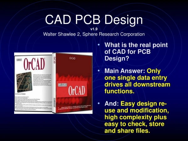
CAD PCB Designv1.9Walter Shawlee 2, Sphere Research Corporation • What is the real point of CAD for PCB Design? • Main Answer: Only one single data entry drives all downstream functions. • And: Easy design re-use and modification, high complexity plus easy to check, store and share files.
CAD PCB Design • On the CAD negative side: It is NOT cheap to commercially acquire (~$1K-15K now typical), or fast to use, and often has a steep learning curve and serious long term deployment problems. • The significantshort term benefits are generally felt to offset these issues in a corporate setting. The continual software upgrade, compatibility, recurrent training and OS headaches never really go away, however. Keeping files usable and users qualified long term is very difficult to achieve.
Manual PCB Design • How was it done before CAD? • Rubylith/Amberlith film, tape, and pads to make over-sized photo-tools. • Resulting boards have a distinct low density appearance. Even double sided art is difficult to align well.
Manual PCB Design • Double sided hand-taped board artwork. • This then created (reduced) photo tools for exposing sensitized PCB material.
CAD PCB Design • How does it work? First, start with a circuit IDEA. • It doesn’t have to be fully developed, this is very important. You can keep modifying and adding throughout the process. • The initial tool to start the idea in the CAD process is called Schematic Capture.
CAD PCB Design • The Schematic Capture phase associates PARTS (symbols) with a specific pin-by-pin interconnection, that association forms the NET LIST.
CAD PCB Design • Each PART is also associated with a physical FOOTPRINT. This data, coupled with the NET LIST make it possible to create a printed circuit board or PCB.
CAD PCB Design • There is an almost infinite variety in terms of PARTFOOTPRINTS. A resistor can be through-hole or surface mount, and can come in almost any size and shape.
CAD PCB Design • Any given schematic could produce many boards, simply by altering the FOOTPRINT of each part or its value to suit a given application…
CAD PCB Design • All too often, the parts needed DO NOT EXIST in the CAPTURE software, then the LIBRARY EDITOR must be used to create them. • This is a major roadblock in all CAD software, and a significant delay to using new parts.
CAD PCB Design • Poor LIBRARY EDITOR functions, or library errors can dramatically slow down CAD designs. • Weak, incomplete, inconsistent or incorrectLIBRARIES are the perpetual problem of all PCB CAD software. 1-2, 2-1, A-C, A-K, anode, cathode issues remain everywhere.
CAD PCB Design • Common library problems include mismatched connection points, wrong hole sizes, missing pins, incorrect sizing, lack of polarization marks and much more. • It is easy to make new parts, but it is not a quick process to do it well, and Spice data cannot be done by the user, thus halting simulation.
CAD PCB Design • If the CAPTURE program does not internally link to and store the FOOTPRINT data, then moving the files to another computer with a different library may be problematic. • The ideal situation is to have project files which are internally self-sufficient, and compatible shared libraries between users.
CAD PCB Design • The next step in the CAD PCB process is to take the data generated from the SCHEMATIC CAPTURE, and feed it into the next program process, which is the PCB LAYOUT TOOL. In addition, a BOM or bill of material can be generated for purchasing and production, listing all the parts and their identifiers or IDENTS. • LAYOUT will automatically take the physical data (net list & footprints), and create a “rat’s nest” basic layout.
CAD PCB Design • The Rat’s Nest simply tosses all the footprints onto the workspace and shows where connections should go. The rest is up to you.
CAD PCB Design • The Rat’s Nest can ALSO contain some design tool features, stored in a Technology File or other predefined Template. • These can include colors, layers, required symbols, tables, predefined board outlines, etc.
CAD PCB Design • Going from the Rat’s Nest to a usable board requires: • A defined Board Size • A layout Strategy • Design Rules • Physical Routing
CAD PCB Design • Board Size (or at least a defined area) is needed to allow Autorouting or Pouring. You have to determine the size, or just let it flow naturally from the layout as it progresses. • Size can be changed at any time, and is not really important until the end, and as needed to fit any specific project requirements.
CAD PCB Design • Board Strategy is how you intend to order the parts on the board, how you want it to look, andany issues you think are important for a workable design. • Many boards turn out poorly because too little forethought goes into them. Think through assembly, test and end use carefully.
CAD PCB Design • Board Strategy may dictate sensitive part separation, the use of large areas for heat sinks, shields, or require careful control or partition of power and ground traces or pours for minimum signal noise and radiated emissions in the final design.
CAD PCB Design • Good Strategies include: • The use of large planes (pours) for power and ground to reduce supply noise and reduce emissions. Insure adequate trace width for power and ground paths. • Partitions of ground and power to keep digital noise from sensitive analog sub-systems. • Clean signal flow from inputs to outputs.
CAD PCB Design • Good PCB Design is ART, it transcends simple technical skill in exactly the same way a good book is not simply the use of language. • This skill improves with use and the study of other good work. You will know your work is of good quality when other people start to copy the way you work.
CAD PCB Design • Use Thermal Reliefs to attach parts to heavy tracks and fills or soldering may become impossible. • Document and mark EVERYTHING both on the board and the schematics.
CAD PCB Design • Design Rules set key factors like minimum track size, track to track and pourspacing, via definitions, and other variables that can be controlled and defined globally in the design. • Mistakes here can make the design very difficult, so think about what will work best for this task. These are set by you, but are controlled in software.
CAD PCB Design • Routing can be done by you manually, a track at a time, or to some degree by Auto-routing (if available). • Auto-routing is best for logic array or memory wiring where there are repetitive patterns, but is not very effective in analog design.
CAD PCB Design • Routed boards have LAYERS, representing copper, silk screens, solder masks, outline information, drill information and assembly data. • You can only really see and work on one layer at a time, because they are visually stacked on top of each other like pages in a book.
CAD PCB Design • Layers have unique names, somewhat standardized over time, they are (in sequence): • TOP SILK SCREEN,TOP SOLDER MASK, TOP,POWER,INNER1-16,GROUND,BOTTOM,BOTTOM SOLDER MASK,BOTTOM SILKSCREEN. • Colors are not standardized, but a black background workspace is much easier on your eyes than white. The associated layer Gerber Files DO have standardized names.
CAD PCB Design • Once the board is routed, checked (use any DRCDESIGN RULE CHECKING features available), all cosmetic features touched up and reviewed by another person, then you can go to the production phase. Peer review is critical to catch errors. • For PCB production, you can run the Gerber Post-Processor from the LAYOUT tool to generate Gerber files, drill charts and design files. Purchasing and assembly get the BOM or Bill of Materials file.
CAD PCB Design • Gerber Files contain the layer-by-layer data plus the drill info and outline to make a finished PCB. • Make sure you have EVERY FILE required, and none that are not required, then add any needednotes, and archive to send out for board manufacturing.
CAD PCB Design • Gerber Files drive a Gerber (or other) photoplotter which makes the PHOTOTOOL to expose the sensitized PCB material or screen and mark pads and tracks. • The Drill File runs an Excellon (or other) automated drill which matches hole sizes to locations, and drills the board.
CAD PCB Design • The CAD PCB work flow is shown at left, red paths are manual, blue are automated. • Some programs also support Back-Annotation, where a change made downstream will automatically reflect back to the source files.
Common CAD Tools • Protel and the later AltiumDesigner platform from Altium. • Cadence Orcad. • CadSoft Eagle. • Mentor Graphics PADS. • Public Open Source (no charge) tools: DesignSpark, KiCAD, PCB123, ExpressPCB
CAD PCB Design Tips • Cost is directly proportional to size, layers, holes and speed of delivery. • Single sided boards are cheap, but solder joints are very weak mechanically. Double sided board production has become the default industry standard, with plated through holes. • Adding each pair of additional layers more than doubles costs, and may require electrical testing, another cost adder.
CAD PCB Design Tips • Copper thickness is 1 oz (per sq.ft.) standard, for more current, it is usually plated up during the double sided process. • Thickness: • ½ oz.= 0.7mils • 1 oz.= 1.4mils • 2 oz.= 2.8mils
CAD PCB Design Tips • Surface finishing has changed considerably in the post-RoHS world. • HASL tin-lead solder was standard for many years, but is now being replaced with other enviro-friendlier finishes including tin, silver and ENIG (electroless nickel, immersion gold). • A process called SMOBC is also possible (solder mask over bare copper), with plating only at pads for soldering.
PCB Extras • Most boards now have a SOLDER MASK, usually applied to both sides. This is to improve solderability (reduce bridging), and to prevent corrosion after manufacture, defined in Gerber Files.SMT, SMB. • Boards also typically have IDENTS, to mark parts and locations, generally in silk-screened epoxy inks, on one or both sides, also defined in Gerber Files. SST, SSB. • SMD boards may also have SOLDER PASTE tools, made in a separate metal stencil, for the screening of solder paste for assembly, also defined in Gerber Files. SPT, SPB.
Standards • Association of Connecting Electronics Industries IPC-2221/A/B. This is a total design guide for aspects of layout and manufacturing. • MIL-STD-275E, MIL-PRF-31032B, IEC-60297-3 (Eurocard) and IEEE 1101.10 • Most are now already uploaded to the study files area to review.
General Design Tips • We keep a large reference page at Sphere Research where you can often find very useful design information links, it is located here: • http://www.sphere.bc.ca/test/data.html
You Should Read: • Donald A. Norman’s “The Design of Everyday Things”
You Should Read: • W. Edwards Deming’s “Out Of The Crisis”
And possibly: • “1 boat” • http://www.sphere.bc.ca/document.html
Thank you! • Class materials are at: http://www.sphere.bc.ca/class