Download

1 / 35
350 likes | 425 Vues
Develop a Data Acquisition Board (DAQ) using ADS1278 ADC and THS452X op-amps for precise sampling of analog channels. The board will be designed as a multipurpose tool with modularity allowing custom configurations. Explore manufacturing options and finalize schematic for simulation in TINA-Spice.

E N D
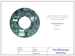
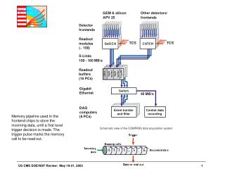
DAQ PCB Design Kory
Goals • Develop a Data Acquisition Board (DAQ) using the ADS1278 ADC and the THS452X op-amps that will condition and sample 8 analog channels synchronously. • The board will connect directly to the myRIO through a 32 pin MXP providing all of the necessary power and data transmission lines. (SPI, SCLK, etc.) • The board will be designed as a multipurpose precision DAQ that can sample up to 151 ksps of 24 bit data. • The board will provide some modularity where AA filters may be disabled and potentially a PGA could be on board providing user selection
To DO • Find out if BatchPCB populates boards or go with a local manufacturer • Decide differential approach or single ended. • Finalize Schematic and simulate in TINA-Spice
Important Links Forum e2e Post *** ADS1278 Data Sheet EVM ADS1278 User Manual THS452X Amp Data Sheet THS452X EVM Manual ADS127L01 24-Bit, High-Speed, Datasheet
More Design Links https://e2e.ti.com/support/amplifiers/high_speed_amplifiers/f/10/t/631113?tisearch=e2e-sitesearch&keymatch=ths4521 https://e2e.ti.com/support/amplifiers/high_speed_amplifiers/f/10/t/669153?tisearch=e2e-sitesearch&keymatch=ths4521%20ads1278 ECG reference Design Analog Engineer’s Pocket Reference** TI Precision Labs Lecture Manual** Precision Labs **
More Resources delta-sigma ADC basics Data Converters – Learning center** Understanding input range requirements for Precision ADCs with integrated PGAs Delta-sigma-advantage-to-anti-aliasing-filters Benefits of Delta-Sigma Analog-to-Digital Conversion
Ref. Projects with Schematics • ADS1278 EVM • Electret Pre-amp • THS452X EVM • ADS127L01 Delta-Sigma ADC • Quad-Channel 250-Msps Digitizer with Variable Gain Amplifier Reference Design -Low Power, Low Noise 24b Analog Front-End 8-ch Isolated High Voltage Analog Input Module High Accuracy Analog Front End Using 16-Bit SAR
TI Reference Design Video elecret amp board http://www.ti.com/tool/ads127l01evm DigiKey Ref Design
Voltage Regulator TI Reference Designs TI's List http://www.ti.com/power-management/reference-designs.html https://www.baldengineer.com/regulator-basics.html Popular LDO SC LDO Need 1.8V and 4.5uA, max 5.1 on plugin ch1,
Potential Components LDO, Report (Low-noise Power) Pre-amplifiers Audio Op-Amps and references** Step Down Converter Electret Microphone Amplifier - MAX9814 with Auto Gain Control SparkFun Electret Microphone Breakout SparkFun MEMS Microphone Breakout - INMP401 (ADMP401)
Potential Eval Hardware TI Precision Amplifier Quickstart Kit TI Precision Labs - Op Amps Evaluation Module THS4521EVM User Guide DataSheet MEMS Mic > ECM
Scratch Notes • Should I include aPGA? • Check out this reference design that includes AA-filters(More links in TI notes slide)** • Single supply or dual? • Analog Engineer’s Pocket Reference • ADS1x7x Excel™ Calculator Tool • TI DelSigma • Data Converters – Learning center • TI Precision Labs
Companion to ADS1278 THS4521 LP5907 TL431A
Where to order PCB? https://oshpark.com/(BatchPCB) -https://dorkbotpdx.org/wiki/pcb_order https://dirtypcbs.com/store/pcbs http://www.4pcb.com/ https://www.expresspcb.com/ http://www.sunstone.com/pcb-products/assembly-services Oregon These high quality boards do not include the silkscreen or solder mask layers.
Chinese Manu. https://www.pcbcart.com/ https://www.pcbgogo.com/ https://www.pcbway.com/
Notes from TI guides etc 2.5 Layout Considerations Board layout is critical for high-speed circuits. To achieve a proper layout, TI recommends the following: • The amplifier and ADC should be located as close together as possible to reduce effects of impedance mismatch and minimize inductance. • Both the amplifier and the ADC require that the filter components be located in close proximity. • The ADC digital outputs must be well isolated from the ADC input as well as from the amplifier inputs. • The amplifier input and output pins should not be placed over power or ground planes to reduce parasitic capacitance for stability reasons. • Power-supply bypass capacitors should be low ESR and placed within 2 mm of the associated pins. • When vias are used, using multiple vias is recommended. This includes placing ground vias near vias on the signal traces. source**, datasheet
Notes from TI guides etc Spurious-free dynamic range (SFDR) is the strength ratio of the fundamental signal to the strongest spurious signal in the output. It is also defined as a measure used to specify analog-to-digital and digital-to-analog converters (ADCs and DACs, respectively) and radio receivers. SFDR is defined as the ratio of the RMS value of the carrier wave (maximum signal component) at the input of the ADC or output of DAC to the RMS value of the next largest noise or harmonic distortion component (which is referred to as a “spurious” or a “spur”) at its output. SFDR is usually measured in dBc (i.e. with respect to the carrier signal amplitude) or in dBFS (i.e. with respect to the ADC's full-scale range). Depending on the test condition, SFDR is observed within a pre-defined frequency window or from DC up to Nyquist frequency of the converter (ADC or DAC) brief review of op-amps
Design Software • Downloaded Eagle and Circuit Maker, I will first be looking at designing in CM • Also could do ExpressSchematic and ExpressPCB • TI Filter Designer
Circuit Maker Introduction Links • https://documentation.circuitmaker.com/ Top Level • https://circuitmaker.com/forum/posts/220414 • http://documentation.circuitmaker.com/display/CMAK/From+Idea+to+Manufacture+-+Driving+a+PCB+Design+through+CircuitMaker • http://documentation.circuitmaker.com/display/CMAK/Exploring+CircuitMaker • Youtube Intro • Video Gallery
Notes From TI Blog Post your AAF should attenuate the noise seen after the first Nyquist frequency to a level which is insignificant when compared to the ADC's inherent quantization and thermal noise For a SAR, this attenuation level must be reached very close to Nyquist. However, for a delta-sigma ADC, this attenuation is really necessary closer to the modulator sampling frequency (fMOD). Between the data rate Nyquist frequency (fDATA / 2) and fMOD, the digital filter stopband will suppress most of the out-of-band noise. The signal bandwidth of interest determines the passband that you need for your filters (AAF and digital). The difference in frequency between the signal bandwidth and the aliasing band determines the type of AAF and the response you need. Ideally, your AAF and digital filter should remain relatively flat throughout your bandwidth of interest. For low-speed applications where the bandwidth is only a few hundred hertz, a first- or second-order RC filter may be enough since the modulator of the ADC is often running at frequencies greater than hundreds of kilohertz. Conversely, a high-speed application with hundreds of kilohertz of signal bandwidth may need a high-order active filter to reach the attenuation target before a modulator frequency of a few megahertz.
https://www.planetanalog.com/document.asp?doc_id=532470&site=planetanaloghttps://www.planetanalog.com/document.asp?doc_id=532470&site=planetanalog Delta-sigma ADC signal chain The signal chain for the delta-sigma converter application starts with the sensor (left side of Figure 1). Contrary to a typical SAR-ADC system, there are no analog gain circuits, such as an amplifier and instrumentation amplifier, following the sensor block. Between the sensor and the delta-sigma converter, there is an anti-aliasing, low-pass filter. The delta-sigma converter and the SAR-ADC anti-aliasing filter designs are significantly different. With a SAR converter, the anti-aliasing filter usually has an active fourth to eighth order implementation, requiring two to four amplifiers. As Figure 1 shows, the delta-sigma anti-aliasing implementation generally requires only a first order, passive filter [1]. With the digital filter in place, the requirements placed on the anti-aliasing filter become even more relaxed! Instead of needing to filter everything beyond the Nyquist frequency as in SAR ADCs, the anti-aliasing filter for delta-sigma ADCs only needs filter out unwanted frequency content around multiples of fMOD. This allows for an even more gradual filter roll-off that is much easier to design with a few discrete, passive components. Typically, a single-pole RC filter is all that is required, but you may need a second-order filter for lower OSRs.
TI Filter Designer Resources - Videos
Hardware/Connectors DIN 41651 PCB connectors (MXP is 0.1”) https://store.digilentinc.com/mxp-extender-cable-for-myrio/ https://www.digikey.com/product-detail/en/te-connectivity-amp-connectors/1-215307-7/A121775-ND/2278494 Soldering SMA Female PCB SMA Cable Male Connectors SparkFun MEMS Microphone Breakout - INMP401 (ADMP401)