Quantum Enabling Technology Materials Research for Superconducting Quantum Computing
Quantum Enabling Technology Materials Research for Superconducting Quantum Computing. Materials P.I. - D. P. Pappas Affiliates: Jeff Kline Fabio da Silva Students: Will Kindel Teresa Osminer Postdocs *David Wisbee. Anatomy of a superconducting qubit. Wiring. Top electrode.

Quantum Enabling Technology Materials Research for Superconducting Quantum Computing
E N D
Presentation Transcript
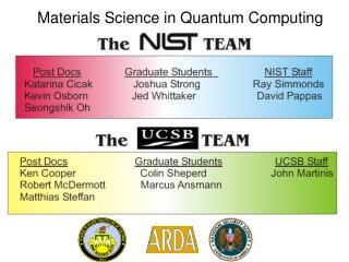
Quantum Enabling TechnologyMaterials Research for Superconducting Quantum Computing Materials P.I. - D. P. Pappas Affiliates: Jeff Kline Fabio da Silva Students: Will Kindel Teresa Osminer Postdocs *David Wisbee
Anatomy of a superconducting qubit Wiring Top electrode Insulator Junction - Tunnel barrier Bottom electrode Insulator (if subs. conductive) Substrate
Materials development – can we reduce decoherence? Al a-SiOx Absorption in dielectric & junction (a-SiO2) & (a-AlO2) AlOx Si • Focus on: • Insulators: along traces & around junction • in substrate • crossovers • Tunnel barrier: Between top and bottom electrode • Electrode surfaces: Flux noise from surface spins
Resonant circuits have low Q at low T, P => With & without SiO2 over the capacitor C/2 C/2 L Dissipation is in SiO2 dielectric of the capacitor! ~Pout
Qubit spectroscopysplittings due to two-level systems in Junction tunnel barrier • Increase the bias voltage (tilt) • Frequency of |0> => |1> transition goes down Increase bias Resonances
DC SQUIDs: SF1/2(1Hz) vs. T Loop materials: Nb (A1-4, F1) Pb (C2) PbIn (A5, B1, C1, E1,2) Loop effective areas: 1,400 mm2– 200,000 mm2 ( At low T: SF1/2(1Hz) ≈ 7 ± 3 mF0Hz-1/2 Wellstood, Urbina and Clarke (1987)
Superconducting JJ qubits – mtls. & meas. Primary NIST differentiator – Crystalline junction material Secondary differentiator – Crystalline bottom electrodes UHV & processing combination Enabling development: Substrate preparation Development of low loss insulators priority – a-Si:H, a-C:H, Si(111) Benchmarks – a-SiOx, a-SiN Facilities ADR with I/V and RF capablility RF capability on PPMS
Original Statement of Work Tasks: • Substrate preparation • Bottom electrode • Epitaxial barrier development • Top Electrode • Dielectric layers • Top & bottom wiring layers
Progress Studied substrates from different vendors ( collaboration w/LL, DARPA) - Task 1 Obtained 3” wafers of Sapphire (0001) Measured roughness using AFM Developed Qubit test platform for junction tests - Task 1-6 12 qubit test die – quickly find optimized junctions Devices fabricated here Measurements done– 500 ns T1!! Developed insulator test platform – Task 1-6 Make simple structure to test loss in various dielectrics – new set of dies Devices fabricated here Measurements show absorption – sent to JPL Fabricated SQUIDs and measure noise – Task 1-6 Various widths & flux trapping conditions Fabricated Ru capped washers Added Fe Measured - Same noise level with Ru as Al & Re, reduced by factor of 2 0.2 ML Fe Measure junctions in-house for quality control – Task 1-6 ADR test facility built up – Tested first junctions here last week Commissioned 3” chamber for epi Si(111)/Al(111)/Al2O3/Al(111) - Task 1-4
Task 1 - Wafer substrate AFM analysis • Acquired wafers from 3 manufacturers • Epi-stone (ES) & Saint Gobain (SG), and Crystal GmbH (CG) • Conducted AFM on them in collaboration with LL under DARPA • CG & ES wafers looked best – show atomic steps • SG wafer surface looked poor, lots of scratches, no steps. CG wafer surface ES wafer surface SG wafer surface Note – Growth of Re on SG wafers actually show the best RHEED!
Progress Studied substrates from different vendors ( collaboration w/LL, DARPA) - Task 1 Obtained 3” wafers of Sapphire (0001) Measured roughness using AFM Developed Qubit test platform for junction tests - Task 1-6 12 qubit test die – quickly find optimized junctions Devices fabricated here Measurements done– 500 ns T1!! Developed insulator test platform – Task 1-6 Make simple structure to test loss in various dielectrics – new set of dies Devices fabricated here Measurements show absorption – sent to JPL Fabricated SQUIDs and measure noise – Task 1-6 Various widths & flux trapping conditions Fabricated Ru capped washers Added Fe Measured - Same noise level with Ru as Al & Re, reduced by factor of 2 0.2 ML Fe Measure junctions in-house for quality control – Task 1-6 ADR test facility built up – Tested first junctions here last week Commissioned 3” chamber for epi Si(111)/Al(111)/Al2O3/Al(111) - Task 1-4
Qubit loop Bias coil DC-SQUID Task 3 - 12 Qubit Die Layout Allows us to test a wide range of junction sizes even with low yield!
Progress Studied substrates from different vendors ( collaboration w/LL, DARPA) - Task 1 Obtained 3” wafers of Sapphire (0001) Measured roughness using AFM Developed Qubit test platform for junction tests - Task 1-6 12 qubit test die – quickly find optimized junctions Devices fabricated here Measurements done– 500 ns T1!! Developed insulator test platform – Task 1-6 Make simple structure to test loss in various dielectrics – new set of dies Devices fabricated here Measurements show absorption – sent to JPL Fabricated SQUIDs and measure noise – Task 1-6 Various widths & flux trapping conditions Fabricated Ru capped washers Added Fe Measured - Same noise level with Ru as Al & Re, reduced by factor of 2 0.2 ML Fe Measure junctions in-house for quality control – Task 1-6 ADR test facility built up – Tested first junctions here last week Commissioned 3” chamber for epi Si(111)/Al(111)/Al2O3/Al(111) - Task 1-4
Task 5 - Quantum Materials: Low loss insulators Test platform do develop low loss insulators • Collaborating with Ben Mazin to design antenna test platform • Measurements made on a-SiOx as a reference Q ~ 1000 • Just started making measurments on a-ALD-AlOx, • While measurements in progress, preparing SiN, a-C, a-Ge
Progress Studied substrates from different vendors ( collaboration w/LL, DARPA) - Task 1 Obtained 3” wafers of Sapphire (0001) Measured roughness using AFM Developed Qubit test platform for junction tests - Task 1-6 12 qubit test die – quickly find optimized junctions Devices fabricated here Measurements done– 500 ns T1!! Developed insulator test platform – Task 1-6 Make simple structure to test loss in various dielectrics – new set of dies Devices fabricated here Measurements show absorption – sent to JPL Fabricated SQUIDs and measure noise – Task 1-6 Various widths & flux trapping conditions Fabricated Ru capped washers Added Fe Measured - Same noise level with Ru as Al & Re, reduced by factor of 2 0.2 ML Fe Measure junctions in-house for quality control – Task 1-6 ADR test facility built up – Tested first junctions here last week Commissioned 3” chamber for epi Si(111)/Al(111)/Al2O3/Al(111) - Task 1-4
Task 6 - Flux noise vs. F on Ru capped Al with 0.2 ML Fe on top Red curve – SQUID washer w/ Ru cap Blue Curve – Same SQUID washer w/ Ru cap + 0.2 ML Fe on top Factor of 2 reduction in noise due to Fe!! (rather than increasing noise)
Progress Studied substrates from different vendors ( collaboration w/LL, DARPA) - Task 1 Obtained 3” wafers of Sapphire (0001) Measured roughness using AFM Developed Qubit test platform for junction tests - Task 1-6 12 qubit test die – quickly find optimized junctions Devices fabricated here Measurements done– 500 ns T1!! Developed insulator test platform – Task 1-6 Make simple structure to test loss in various dielectrics – new set of dies Devices fabricated here Measurements show absorption – sent to JPL Fabricated SQUIDs and measure noise – Task 1-6 Various widths & flux trapping conditions Fabricated Ru capped washers Added Fe Measured - Same noise level with Ru as Al & Re, reduced by factor of 2 0.2 ML Fe Measure junctions in-house for quality control – Task 1-6 ADR test facility built up – Tested first junctions here last week Commissioned 3” chamber for epi Si(111)/Al(111)/Al2O3/Al(111) - Task 1-4
Results of our junctions: R (1/G) vs. T for Al/AlOx/Al tunnel jctn. • Signatures of quantum tunneling • R increases as T decreases • Zero slope at low T In collaboration with Oh et al (Rutgers) Zero-bias resistance
Progress Studied substrates from different vendors ( collaboration w/LL, DARPA) - Task 1 Obtained 3” wafers of Sapphire (0001) Measured roughness using AFM Developed Qubit test platform for junction tests - Task 1-6 12 qubit test die – quickly find optimized junctions Devices fabricated here Measurements done– 500 ns T1!! Developed insulator test platform – Task 1-6 Make simple structure to test loss in various dielectrics – new set of dies Devices fabricated here Measurements show absorption – sent to JPL Fabricated SQUIDs and measure noise – Task 1-6 Various widths & flux trapping conditions Fabricated Ru capped washers Added Fe Measured - Same noise level with Ru as Al & Re, reduced by factor of 2 0.2 ML Fe Measure junctions in-house for quality control – Task 1-6 ADR test facility built up – Tested first junctions here last week Commissioned 3” chamber for epi Si(111)/Al(111)/Al2O3/Al(111) - Task 1-4
Note: Test devices include all/most layers=> Hard to separate original tasks! • Re-parse SOW Tasks to reflect project goals. • Substrate preparation • Bottom electrode • Epitaxial barrier dev. • Top Electrode • Dielectric layers • Top & bottom wiring • Understand tunneling process • Devices on alternative substrates • Develop high Q circuits • Study noise in devices • Test coherence advances • Still the same scope of work. • Allows us to make Gantt chart directly from SOW.
Detailed subtasks • Understand tunnel process in epi-barriers • Tool up to measure I-V curves in-house with ADR • Measurement of samples at low temperature • Reduce spectroscopy splitting further using different tunnel barriers • Study materials doping in barriers • Study device/junction failure • Develop alternative substrates • Research & indentify new systems • Tool up 3” chamber in clean room for identified system • Prepare substrates • Prepare bottom electrode • Prepare barriers • Prepare top electrode • Fabricate into test junctions • Develop high Q materials for low T, P applications • Tool up for measurements at 1.7 K and 60 mK • Fabricate L-C circuits & test with SiO2 • Tool up to grow a-Si dielectrics • Investigate new materials • Complete work with antenna resonators • Study noise due to surfaces & interfaces • Fabrication of SQUID devices • Identify source of decoherence loss • Test Coherence advances • Fabricate 12 qubit dies using optimal materials from above • Integrate & optimize all improvements into single qubit & measure
