Download
1 / 24
270 likes | 471 Vues
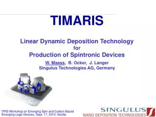
TIMARIS Linear Dynamic Deposition Technology for Production of Spintronic Devices W. Maass , B. Ocker, J. Langer Singulus Technologies AG, Germany. Singulus – The Company. Public traded: SNG

E N D
TIMARIS Linear Dynamic Deposition Technology for Production of Spintronic Devices W. Maass, B. Ocker, J. Langer Singulus Technologies AG, Germany
Singulus – The Company • Public traded: SNG • Employees WW: 572 (Singulus Group at December 31st, 2009; 487 FTE after divestiture of Hamatech APE) • Revenue WW: 116.6 mio € (2009) • Sales/Service: Locations WW • Core Business: Optical Media • Diversification: Solar (Acquisition of Stangl AG) Business Unit Nano Deposition Technologies (NDT) Germany, Kahl am Main near Frankfurt
TIMARIS Motivation: • Essential part of many Spintronic Devices are TMR (or GMR) layer stacks • These layer stacks have to be prepared and manufactured on Ø200mm or Ø300mm wafers • R&D as well as Production related criteria will apply for any deposition tool to be used • The special design of these TMR Layer stacks require a specialized deposition system
Capping Layer (Ta) 2-3 nm 0.8-1.5 nm 0.4-1.5 nm 2-3 nm 0.7 nm 2-3 nm 10-25 nm Seed Layer 2 (NiFe) 2-5 nm Seed Layer 1 (Ta, NiFeCr) 2-5 nm Contact (Cu, Al) 40-60 nm Buffer (Ta) 5-15 nm 2-5 nm MRAM Technology: Field Induced Switching Free Layer 1 (CoFe, CoFeB) Free Layer 2 (NiFe) Barriere (MgO, Al2O3) Pinned Layer 2 (Co60Fe40) Pinned Layer 1 (CoFe) AAF Spacer (Ru) Antiferromagnet (PtMn, IrMn) 8 different materials (or even more ??) in the TMR layer stack ! Production of MRAM and Spintronic Devices on Ø200 mm or Ø300 mm wafers!
TIMARIS: Typical R&D / Production Criteria TMR Wafer Production (MRAM and Spintronic Devices) Requirements for the Deposition Process • Tight Thickness Control of Ultra-Thin Films • Thinnest Film < 0.1 nm; Smallest Thickness Step: < 0.01 nm • Reliable & effective manufacturing of multi – layers of sub – nanometer individual thickness including ferromagnetic films • Very stable and reliable TMR performance High MgO deposition rate • In – situ wafer annealing • Heating up to 600°C and cooling prior to deposition of certain films • Extremely short latency between heating/cooling and deposition • Process advantage for L01 formation in perpendicular TMR designs • High Yield/Wafer by uniform TMR & Magnetic Properties Full flexibility regarding PVD – mode for all targets: DC, pulsed DC, RF • Throughput, Cost of Ownership • Particle, Contamination, ...
TIMARIS: LDD Process technology Deposition technique: Linear PVD Magnetron and linear movement of wafer: Linear Dynamic Deposition (LDD) • Short Target-Substrate Distance: • Good Coating Efficiency • Thickness adjusted by wafer speed: • Tight control & repeatability • Multi-directional coating: • Smooth films and Interfaces • Leakage field of cathode parallel to wafer travel direction: • Ideal symmetry for magnetic film applications • Stationary Aligning Magnetic Field (AMF): • AMF can be optimized with cathode • Robust and reliable design Magnet Array Wafer Sputter Target Deposition Area Wafer Travel Static DepRate
TIMARIS 300/200/150/100mm PVD Bridge System A Proven Deposition Tool for TFH, MRAM and other Semiconductor Applications TIMARIS TIMARIS: 30 years of Experience In its history the NDT team has designed, built and run different types of production tools (PVD, IBD, CVD) for • Thin Film Head Manufactering (e.g. Ferro – Magnetic films and film stacks) • Flat Panel Display (large area deposition) • Semiconductor (e.g. Metallization)
TIMARIS: Photography Multi Target Module Top: Target Drum with 10 rectangular cathodes; Drum design ensures easy maintenance; Bottom: Main part of the chamber containing LDD equipment RF – Equipment (Match – Box, RF - Switches) Soft-Etch Module(PreClean, Surface Treatment) Transport Module(UHV wafer handler MX700) Cassette Modules(according to Customer request) Ultra – High – Vacuum Design: Base Pressure 5*10-9 Torr (Deposition Chamber) High Throughput: 10 Wafer/Hour (NiFe 2.5nm/CoFe70 250nm) High Tool Availability: Maintenance friendly Design High Reliability: Solid and Well Engineered Design Up-Time: 90%, MTBF: 150h, MTTR: 3h
TIMARIS: Example for Layout Tool Configuration for advanced Thin Film Head or Semiconductor R&D: • Processing of wafers up to Ø300mm 2 x Multi-Target-Modules with 10 Targets each 1 x Combi-Process-Module (CPM) 1 x Rotating Substrate Module (RSM) w/ one PVD and one Ion Source ASYS UHV Transport Module incl. single port EFEM/FOUP 21 PVD cathodes in one system (configuration can be modified according to customer request)
TIMARIS: Modularity Rotating Substrate Module (RSM): • Rotating substrate deposition • Tilting of substrate wrt. process direction • Multiple process options depending on the installed process equipment (not all of the shown options can be combined): • Up to six (6) PVD cathodes (DC, pulsed DC, RF), target diameter 125mm (5”) or below w/ cathode shutters • Up to two (2) PVD cathodes (DC, pulsed DC, RF), target diameter 320mm (12”) w/ cathode shutters • One (1) Ion source according to specification • Thin film characterization metrology • Substrate heating (up to 450°C) • Remote plasma / Natural (O2) oxidation • Co – sputtering • Con – focal sputtering • Cathode – Substrate – Distance can be changed (by adapter) • Base pressure 10-8 Torr • In-situ Aligning Magnetic Field (1 RSM module in design phase to be manufactured)
CoFe Seed TIMARIS: LDD Process technology Magnetic Requirements: Alignment across Wafer Specification: Easy Axis deviation < +/- 2° Example: Seed/Fe70Co 250nm MOKE measurements, 49 points, Measured alignment of the Easy Axis across wafer: TIMARIS Real Measurement Ideal Situation
CoFe Seed Comparison with Competition Process technology by Circular Cathodes Example: Seed/Fe70Co 250nm deposited not by TIMARIS MOKE measurements, 49 points, Alignment of the Easy Axis across wafer Remark: The shown data are to demonstrate the principal issues related with the discussed deposition technology. It is not argued, that certain process results cannot be achieved at all with the respective technology! Real Measurement
TIMARIS: MgO – TMR, Summary MgO – Barrier, TMR vs. RA: Typical layer stack: Ta5/PtMn20/CoFe2.3/Ru0.8/CoFeB2.2/MgO1.2/CoFeB3.0/Ta10 (nm)
5Wµm²: (Lead: 5 Ta / 50 CuN / 3 Ta / 50 CuN) RA uniformity : 3.8% (1) MR uniformity : 3.2% (1) MgO : thickness: 0.84 nm th. uniformity: 0.025 nm (MaxMin) th. uniformity: 0.61% (1) 26Wµm²: (Lead: 5 Ta / 30 CuN /) RA uniformity : 4.1% (1) MR uniformity : 2.8% (1) Ø300mm MgO : thickness: 1.06 nm th. uniformity: 0.03 nm (MaxMin) th. uniformity: 0.53% (1) perpendicular parallel TIMARIS: Uniformity of RF sputtered MgO 3 Ta / 16 PtMn / 2.5 CoFe30 / 0.85 Ru / 2.4 Co40Fe40B20 / rf-MgO / 2.0 Co40Fe40B20 / 10 Ta RA: 2.9% RA: 3.2% RA: 3.7% RA: 4.3% Annealing: 1.0 Tesla, 360°C, 2h
Perpendicular Magnetic Anisotropy (PMA) PMA: Sub / Seed / [Co (0.3nm)/ Pd (1.0nm)] x 3/ Ta (10 nm) VSM measurements Field annealing: 1.0 Tesla, 300°C, 2h Perpendicular to plane In-plane TIMARIS: very tight control of Co and Pd thickness to adjust perpendicular anisotropy
TIMARIS: MgO – TMR, Wedge Technology Deposition of Wedge-Films by LDD Technology Variable film thickness across wafer for thickness optimization by changing wafer speed during deposition. Range 1.0nm to 2.0nm is example only !!
TIMARIS: MgO – TMR, Wedge Technology Layer stacks: Etch/5Ta/50CuN/3Ta/50CuN/3Ta/16PtMn/2CoFe30 /0.9Ru/2.3Co40Fe40B20/wedge MgO/2.3Co40Fe40B20/ 10Ta/30CuN/7Ru (nm) Co40Fe40B20 (A), (B) Etch/5Ta/45CuN/3Ta/45CuN/3Ta/16PtMn/2CoFe30 /0.9Ru/2.3Co60Fe20B20/wedge MgO/2.3Co60Fe20B20/ 10Ta/30CuN/7Ru (nm) Wedge Technology: 20 – 30 data points with different MgO thickness by deposition of one wafer only
TIMARIS: Substrate Heating Technology (Patent pending) TMR with Perpendicular Magnetic Anisotropy (PMA) Deposition of different materials on hot substrates: Goal short temperature transitions Principle:
TIMARIS: Substrate Heating Technology (Patent pending) TMR with Perpendicular Magnetic Anisotropy (PMA) Deposition of different materials on hot substrates: Goal short temperature transitions Experimental result (example): • Temperatures up to 450°C • Short heating and cooling time • Heating and cooling within the deposition module resulting in very short latency time between heating/cooling and deposition Closed loop ctrl Heater ON
TIMARIS: Substrate Heating Technology (Patent pending) Heating Experiments : Conditions: • Substrate: Ø200mm Si wafer • Extra data point: 100nm Ru coated( not calibrated) • Power of heater: 50% • Temperature start point: 100°C • Closed loop control: not optimized Short temperature rise time
TIMARIS: Substrate Heating Technology (Patent pending) Heating Experiments : Temperature rise time, effect of coating: Conditions: • Substrate: • Ø200mm Si wafer • Ø200mm Si wafer + 100nm Ru( not adjusted) • Temperature start point: approx. 100°C • Closed loop control: not optimized
TIMARIS: Substrate Heating Technology (Patent pending) Heating Experiments : Cooling after heating Conclusion: • Temperature drop has to be considered • Deposition of approx. 3nm of ferromagnetic material can be done in ca. 15 sec. Conditions: • Substrate: Ø200mm Si wafer
TIMARIS: Gradient Concentration Alloy films (Patent pending) Adjustment of alloy concentration for TMR films with Perpendicular Magnetic Anisotropy (LDD – Technology) Deposition of FexPd(1-x) or FexPt(1-x) as well as other alloys requires in many cases a carefully adjustment of the material concentration to get the best device performance. TIMARIS’ “Gradient Concentration Alloy” capability allows to deposit films on wafers with varying concentration across the wafer. The gradient of this concentration variation can be adjusted. Fe - rich Pd - rich