Download
1 / 36
360 likes | 484 Vues
This project focuses on implementing the Rijndael AES encryption algorithm on chip for integrated circuit design, aiming for high performance and efficient encryption processing. The design involves critical components such as sub-ROMS, key D flip-flops, and optimal routing strategies. Key objectives include achieving a throughput speed of at least 350 MHz, maintaining a 1:1 size ratio, and ensuring the security of private keys stored in hardware. The current project status includes proposals, layout designs, simulations, and ongoing resolutions of timing and routing challenges.

E N D
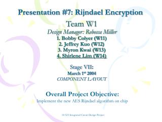
Presentation #7: Rijndael Encryption Team W1Design Manager: Rebecca Miller1. Bobby Colyer (W11)2. Jeffrey Kuo (W12)3. Myron Kwai (W13)4. Shirlene Lim (W14) Stage VII: March 1st 2004 COMPONENT LAYOUT Overall Project Objective: Implement the new AES Rijndael algorithm on chip 18-525 Integrated Circuit Design Project
Status • Design Proposal • Architecture Proposal • Size Estimates/Floorplan • Gate Level Design • Layout • Component Layout • Simulations • To be Done • Top Level Routing • Optimizations • Everything else… 18-525 Integrated Circuit Design Project
Design Decisions & Problems • DECISIONS • Split ROM • Added logic because of split rom • Split into 4 sub-ROMs • PROBLEMS • Timing problems • Routing Problems – Global Level • Sizing of DFF to get equal rise and fall times 18-525 Integrated Circuit Design Project
Project Goals & Objectives Implementing Rijndael Encryption on Chip with this in mind: Throughput Speed At least 350 Mhz Size As dense as possible while maintaining a ratio of 1:1 18-525 Integrated Circuit Design Project
Project Goals & Objectives On-Chip Encryption to be used in: Web servers High through put for passing through information Hardware encryption generally 10-100x faster than software Security of a private key greater if stored in hardware Software keys can be hacked, stolen and used elsewhere 18-525 Integrated Circuit Design Project
TOP LEVEL SCHEMATIC
Updated Floorplan 325 um x 330 um Metal 4 Key DFFs and Input Logic 5th Round Key Expand SBOX and Control Logic Metal 3 Metal 2 Input to SBOX Logic & Select Output and Input Logic Metal 1 4 Rounds of Key Expand CLK Divider 4 Rounds of Round Permutation Input/Output Logic Select & Input Logic Text DFFs and Add RoundKey Final Text Out SBOX and Control Logic
Round Permutation & DFF
D-FLIP FLOP LAYOUT 18-525 Integrated Circuit Design Project
Waves D-FlipFlop Fall Time 531.818p 624.832 ps 18-525 Integrated Circuit Design Project
Waves D-FlipFlop Rise Time 1.08073 ns 502.778p 18-525 Integrated Circuit Design Project
Waves D-FlipFlop Propagation Time 416.542p 1.15726 ns 18-525 Integrated Circuit Design Project
DFF Setup Time 100.237p 408.723p 174.371 ps 18-525 Integrated Circuit Design Project
ROM Propogation Time 408.723p
Critical Path 1.03n 245.367 ps 18-525 Integrated Circuit Design Project
More on Critical Path • Must include the setup time for DFF • Actual Critical Path is about 1.2n • Must double it as this logic only occurs on negative edge of clock • Speed Estimation: 417MHz
Questions? 18-525 Integrated Circuit Design Project