Materials & Processing for Si Compatibility
This workshop overview presents advancements in photonic bandgap (PBG) materials suitable for optical interconnects crucial for high-performance computing. Discussions focus on hard dielectric waveguides, compatibility with low-loss optical fibers, and polymeric waveguides. Key technologies include LPCVD-based buried BPSG/TEOS and SiON for high-density routing. The challenges in microfabrication, including precision stacking and planarization, are addressed alongside applications in millimeter-wave frequencies. Simulated transmission efficiencies and innovative PBG structures are explored for efficient on-chip communication.

Materials & Processing for Si Compatibility
E N D
Presentation Transcript
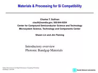
Materials & Processing for Si Compatibility Charles T. Sullivan ctsulli@sandia.gov, 505/844-9254 Center for Compound Semiconductor Science and Technology Microsystem Science, Technology and Components Center Shawn Lin and Jim Fleming Introductory overview Photonic Bandgap Materials Optical Interconnects for High Performance Computing Workshop Oak Ridge 11/8-9/99
Possible Options for On-Chip Waveguide Interconnects • Hard dielectric waveguides • low-loss optical fiber compatibility • low index contrast N ~ 0.005 • = 0.1 dB/cm to < 0.01 dB/cm • e.g., LPCVD-based buried BPSG/TEOS • higher-index for higher-density routing • high index contrast N > 0.1 • < 0.1 dB/cm ? • e.g., LPCVD-based SiON/TEOS • Polymeric waveguides • low-temperature post-processing • low index contrast N ~ 0.05-0.005 • ~ 0.1 dB/cm to 0.5 dB/cm, depending on • e.g., fluorinated acrylates or polyimides
Possible Applications of PBG Materials Bandstop is Largely Independent of Angle Transmission Wavelength (m)
Simulated Electric Field Patterns for90-degree Waveguide Bend 2D Square Lattice 3D Square Lattice
1.2 1.0 theory 0.8 experiment 0.6 Transmission Efficiency 0.4 0.2 0 75 80 85 90 95 100 105 110 Frequency (GHz) 90-degree Waveguide Bend at Millimeter-Wave Frequencies
The Microfabrication Challenge The minimum feature size for a lattice with bandgap of 1.5 micron is 0.18 microns!
3D Silicon Photonic Crystal at Mid-IR Frequencies Technology Challenges - precise stacking; - smooth planarization; - large area uniformity. Top View Side View poly-Si Si substrate 4-layer crystal
Measured Results bandgap 100 3L 4L Transmission Efficiency 20 1.7 1.4 1.6 1.8 1.5 1.3 Wavelength (m) 1.5µm Bandgap Fillet Structure
Defect Volume: 0.23 Modal Volume: 0.8l3 7 6 5 6.4m (0.6) 4 3 2 1 9.2m (0.8 ) Singlemode 3D Defect Cavity Higher-Q Results

