New Vendor for High Volume Production of Silicon Particle Detectors
380 likes | 493 Vues
This project overview highlights the collaboration and progress in the production of silicon particle detectors, essential for high-energy physics experiments. We discuss the evolvement of silicon sensor technology, from its inception in the 1950s to the integration of new vendors like Infineon, who are poised to enhance large-scale manufacturing capabilities. The ongoing electrical characterization, beam tests, and production batches demonstrate our commitment to quality and innovation. This work aims to meet the growing demands of experiments like those at CERN's CMS and ATLAS upgrades.

New Vendor for High Volume Production of Silicon Particle Detectors
E N D
Presentation Transcript
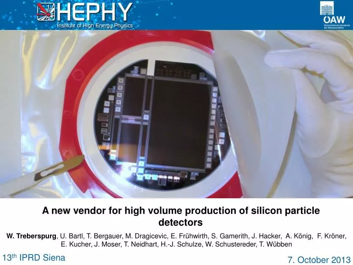
A new vendor for high volume production of silicon particle detectors W. Treberspurg, U. Bartl, T. Bergauer, M. Dragicevic, E. Frühwirth, S. Gamerith, J. Hacker, A. König, F. Kröner, E. Kucher, J. Moser, T. Neidhart, H.-J. Schulze, W. Schustereder, T. Wübben 13thIPRD Siena
Outline Overview of the Project The different Sensor Structures Summary of the Electrical Characterization Summary of Beam Tests Outlook and Summary Wolfgang Treberspurg (HEPHY Vienna)
1. Project Overview: Silicon Sensors • History: • Silicon is used for detectors since the 50ies • Silicon strip detectors have been first used in the CERN experiment NA11 in the 80ies • Today up to 200 m2 (CMS) of silicon sensors are used • The same amount can be expected for the upgrades of CMS and ATLAS • Wafer Size: • NA11 started with 2” and 3” • Today 6” (150 mm) is standard • Introduced in the Industry in the 80ies Wolfgang Treberspurg (HEPHY Vienna)
1. Project Overview: Different Vendors • Small scale R&D production: • Many institutes and companies are able to produce a few 10-100 wafers per year • 6 inch is usually available at many sites • The sensors differ in a broad spectra of quality and price • Large scale commercial production: • Currently only one company is able to produce a few 1.000 – 10.000 high quality wafers per year • Possible new producer: Infineon • Production on thinned 8 inch wafers could be possible Dual or multi-source strategy would be preferable Wolfgang Treberspurg (HEPHY Vienna)
1. Project Overview: Infineon Austria • Villach is aimed for Frontend Production and R&D • The Clean room facilities just extended to over 10.000m2 • Pilot production lines are developed at Villach, E.g.: worlds first power devices on 12 inch wafer (Oct. 2011) • General: Infineon holds 26700 employers at different sites around the world • Villach (Austria): The Austrian site in Villach holds 2400 and produces 50.000 wafer per week Wolfgang Treberspurg (HEPHY Vienna)
1. Project Overview: The Collaboration 1 • End of 2009: Start of project (intense discussion on technical details) • Begin of 2011: Decision of baseline and milestones • Baseline: • Wafer Material: 6” n-type, 300 µm thickness, Approx. 1.2 kΩcm resistivity • Process Specifications: Standard p-on-n technology, AC coupled strips, SiO2/Si3N4 sandwich dielectric, poly silicon resistor biasing • 8 photo masks (one for patterning of Si3N4) Wolfgang Treberspurg (HEPHY Vienna)
1. Project Overview: The Collaboration 2 • August 2011: HEPHY finished the final mask design for the first produced batch • October 2011: Production of the first batch started • April 2012: The wafer have been characterized in Vienna • October 2012: Beam tests and irradiation studies • Beam tests at the SPS accelerator at CERN • Gamma irradiation at SCK-CEN Mol, Belgium • December 2012: Second batch with the same masks and other split groups is produced and delivered in February 2013 • July 2013: Start of irradiation studies with protons (in Karlsruhe at KIT) and neutrons (in Vienna at ATI) • September 2013: Production of third batch with new (modified) masks CMS Track Trigger Prototype Module with 2 Infineon Baby Sensors Wolfgang Treberspurg (HEPHY Vienna)
1. Project Overview: Comments • The production in the clean room was accompanied by our diploma students • The first batch was accompanied by Edwin Frühwirth • The third batch was accompanied by Axel König • We were discussing all technical details directly with the engineers and are involved in the process as far as possible • Since the beginning of 2010 we held weekly telephone conferences • We finally received every wafer from the production batch (except for one wafer, damage due mishandling) • no hidden losses In the cleanroom Wolfgang Treberspurg (HEPHY Vienna)
Outline Overview of the Project The different Sensor Structures Summary of the Electrical Characterization Summary of Beam Tests Outlook and Summary Wolfgang Treberspurg (HEPHY Vienna)
2. Wafer Structures: The STL Sensor • The large standard sensor (STL): • Size: 64 x 102 mm • Active size 61.5 x 99.6 mm • 512 strips (4xAPV) • 120 µm pitch • 20 µm strip implant width • Motivation: • The large sensor has the same dimension as the current CMS sensors Wolfgang Treberspurg (HEPHY Vienna)
2. Wafer Structures: The STS Sensor • The small standard sensor (STS): • Size: 23 x 50 mm • Active size 20.6 x 48.3 mm • 256 strips (2xAPV) • 80 µm pitch • 20 µm strip implant width • Motivation: • The STS sensor is mainly dedicated for building modules • This sensors have been used at tests with a high energy beam Wolfgang Treberspurg (HEPHY Vienna)
2. Wafer Structures: The STI Sensor • The standard irradiation sensor • Size: 7 x 42.5 mm • Active size 5.3 x 40.7 mm • 64 strips (0.5xAPV) • 80 micron pitch • 20 strip implant width • Motivation: • This sensors have been designed for irradiations in the TRIGA Mark II reactor in Vienna with a narrow irradiation tube • The STI sensors have been used for R&D investigations Wolfgang Treberspurg (HEPHY Vienna) 11
2. Wafer Structures: Split Groups • First Batch: • 25 wafers produced with photo masks designed by HEPHY • Wafer 13 not delivered because of mechanical damage • Wafer 04 not diced and used for presentation • Split Groups first Batch: • 23 wafers split into 12 groups to test different process parameters • First split: Gate Oxide (4 groups A to D) • Second split: backside n+ implant diffusion(3 groups A to C) Wolfgang Treberspurg (HEPHY Vienna)
Outline Overview of the Project The different Sensor Structures Summary of the Electrical Characterization Summary of Beam Tests Outlook and Summary Wolfgang Treberspurg (HEPHY Vienna)
3. Electrical Characterization: Measurement Parameter Wolfgang Treberspurg (HEPHY Vienna) • Global parameters: • IV-Curve: Dark Current, Breakdown Voltage • CV-Curve: Depletion Voltage, Total Capacitance • Strip Parameters: • Strip leakage current Istrip • Poly-silicon resistor Rpoly • Coupling capacitance Cac • Dielectric current Idiel
3. Electrical Characterization: Global Values 1/C2 for all large sensors • CV: The depletion voltage of structures on all wafer is around 240 V • IV: In general most sensors feature a low dark current (7 - 30 nA/cm2) • Many Sensors are stable up to 1000 V • Sensors of the X-C split group feature low current but early breakdown STS: ~11 cm2 STL: ~65 cm2 Wolfgang Treberspurg (HEPHY Vienna)
3. Electrical Characterization: The STL Sensor • The plotted values are normalized the median strip value of each sensor • Homogenous values • Accumulation of anomalous strips around strip no. 500 (and 416 for Istrip) • All split groups are affected Rpoly/Rpolymedian Istrip/Istripmedian Cac/Cacmedian Wolfgang Treberspurg (HEPHY Vienna)
3. Electrical Characterization: TheSTS Sensor • Homogenous values • Accumulation of anomalous strips around strip no. 222-248 • Same behavior of anomalous strips as on other sensors • All split groups are affected Istrip/Istripmedian Rpoly/Rpolymedian Cac/Cacmedian Wolfgang Treberspurg (HEPHY Vienna)
3. Electrical Characterization: TheSTI Sensor • Absolute values of measurement plotted • Accumulation of anomalous strips around strip no. 35-55 • Same behavior. • Increasing Istrip • Decreasing Rpoly • Decreasing Cac Wolfgang Treberspurg (HEPHY Vienna)
3. Electrical Characterization: Summary • Criteria: • Istrip > 50 nA (for STL) and Istrip > 25 nA (for STS) • Idiel> 1 nA : short between dielectric and metal strip (Pinhole) • Cac< 1.2 pF: Pinhole • Rpoly: deviation is less than 20% from the median STL: Istrip STS: Istrip • Results STL: • 65 strips of 11776 faulty 5.5‰ • 68% of the faulty strips from area around 500 • Results STS: • 418 strips of 5632 faulty 7% but • 95.3% of the faulty strips from area around 235 • only 22 (3.9‰) outside bad area remain Wolfgang Treberspurg (HEPHY Vienna)
3. Electrical Characterization: Affected Strips 1 • Inter strip measurements on STI sensors: • The inter strip resistance vanishes at affected strips • The inter strip capacitance decreases • A poor strip isolation at this area results in: • Increased Istrip, as the leakage current of more than one strip is measured • The sum of all Istrip currents exceeds the global dark current • Decreased Rpoly, as the bias resistors are some kind of shunted STI STI Wolfgang Treberspurg (HEPHY Vienna)
3. Electrical Characterization: Affected Strips 2 • The accumulation of affected strips is always placed in the same distance to the sensor edge and hence dicing line • STI Sensors of the seconded batch with the same behaviour have been measured • On the undiced wafer in Vienna • The wafer has been sent to Villach (Infineon) for dicing • And has been measured again • The bad area is generated during the dicing process STI STI Wolfgang Treberspurg (HEPHY Vienna)
3. Electrical Characterization: An Explanation • All results indicate an accumulation of charge inside the silicon oxide • Based on that assumption tests with humidity could cure the affected strips • To simulate aging the STI sensor has been exposed 24 h to 180 degree • The sensor still stays cured • The different layer (Implant or Poly Silicon) show no problems STI STI Al Al SiO2 Implant p+ Implant p+ Si n-type Implant n+ Al Wolfgang Treberspurg (HEPHY Vienna)
3. Electrical Characterization: A possible Reason • Bare silicon exposed during later steps of the fabrication • At contact holes in the DC pads • Metal over etch was larger than expected • Bare silicon prone to contamination • Could be the reason for the appearance of charge accumulation • Redesign with corrected overlap of contact holes. The new batch is in production Remark: All layers have been remove by etching for this picture, only bare silicon is left Wolfgang Treberspurg (HEPHY Vienna)
Outline Overview of the Project The different Sensor Structures Summary of the Electrical Characterization Summary of Beam Test Outlook and Summary Wolfgang Treberspurg (HEPHY Vienna)
4. Results of Beam Test: The Setup • 2 detector modules built with STS sensors • 2 detector modules built with strixel sensors • Readout chips (APV25) same as in the CMS tracker • Readout system is a prototype for the Belle II experiment • Detector modules were • Tested at CERN • Gamma irradiated at CNK-CEN Mol • Tested again at CERN Setup at CERN North Area H6 beam line Wolfgang Treberspurg (HEPHY Vienna)
4. Results of Beam Test: Sensor Sections • The bad strip area does not stand out clearly in beam profile and seems to be fully efficient • For a more detailed analysis the sensor has been divided into two sections: • One good section (green) • One bad section (red, strip no. 222 – 238) Wolfgang Treberspurg (HEPHY Vienna)
4. Results of Beam Test: Different Sections • The results indicate problems with the strip isolation at the “bad area” • Clusters are wider in “bad section” • The eta distribution indicates an anomalous charge sharing between the strips Wolfgang Treberspurg (HEPHY Vienna)
4. Results of Beam Test: Gamma Irradiation • The modules have been gamma irradiation and tested again • The gamma irradiation mainly effects the silicon oxide layer on the sensor surface • Gamma irradiation seems to cure the problem, which fits well to the assumption of accumulated charge inside the silicon oxide Results just from “bad area” Gamma Irradiation Wolfgang Treberspurg (HEPHY Vienna)
Outline Overview of the Project The different Sensor Structures Summary of the Electrical Characterization Summary of Beam Tests Outlook and Summary Wolfgang Treberspurg (HEPHY Vienna)
5. Summary: Beam Test and Characterization • A very first prototype batch of planar p-on-n sensors was produced at Infineon-Villach • The STS sensors show reasonable performance. They have very uniform noise and a standard cluster width- and eta distribution. • Electrical characterisation show promising quality • We found areas of strips which behave abnormal • A possible explanation for this effect has been suggested • The explanation will be tested with a new batch of sensors Noise of STS Cluster width of STS (including the “bad area”) Wolfgang Treberspurg (HEPHY Vienna)
5. Summary: Outlook • Irradiation tests: • The reactor in Vienna (neutrons) became operational again • The irradiation at Karlsruhe (protons) is in progress • Producing a new batch: • Three masks have been redesigned with small corrections to prevent the “bad strip area” • The production is in progress and the sensors will be delivered in the next months • New run planned with CMS in 2014: • According to the CMS baseline n-on-p process on 200 µm FZ material • Production on 8 inch wafers is considered • Infineon could be a future supplier of high quality silicon sensors for large scale applications • ATLAS and CMS already show an interest in the possibilities offered by Infineon Wolfgang Treberspurg (HEPHY Vienna)
ThankS for your attention! Wolfgang Treberspurg (HEPHY Vienna)
Backup Slides: Electrical Strip Parameter 1 Detector at a reverse bias of 300V • Strip LeakageCurrentIstrip • Electrometer connected to DC pad measures strip current for each strip • Poly-silicon Resistor Rpoly • Resistance measurement between bias-ring and DC pad • Coupling Capacitance Cac • Capacitance of dielectric between Al strip and strip implant • Dielectric Current Idiel • Current through dielectric at 10V between Al strip and implant Wolfgang Treberspurg (HEPHY Vienna)
Backup Slides: Electrical Strip Parameter 2 STS Idiel/Idielmedian Pinholes STL STS STL Idiel/Idielmedian Wolfgang Treberspurg (HEPHY Vienna)
Backup Slides: Strip Classification • Criteria STL: • Pinhole: short between dielectric and metal strip (Idiel > 1nA) • Coupling capacitance: Cac < 1.2pF • Single strip current: Istrip > 50nA • Polysilicon resistor: more than 20% deviation from the median • Criteria STS: • Pinhole: short between dielectric and metal strip (Idiel > 1nA) • Coupling capacitance: Cac < 1.2pF • Single strip current: Istrip > 25nA • Polysilicon resistor: more than 20% deviation from the median With “bad Area” Without “bad Area” Wolfgang Treberspurg (HEPHY Vienna)
Backup Slides: Long term Stability • Vbias=300V, temperature ~19 °C, rel. humidity 6-50% • Leakage Current stable for all sensors tested Wolfgang Treberspurg (HEPHY Vienna)
Backup Slides: Additional Beam Test Results Resultsfrom „good“ striparea Resultsfrom „bad“ striparea CW1: SNR 32 CW2: SNR 24 CW3: SNR 21 CW1: SNR 32 CW2: SNR 22 CW3: SNR 19 Signal-to-Noise CW1 CW2 CW3 CW1 CW2 CW3 Cluster Signal Wolfgang Treberspurg (HEPHY Vienna)