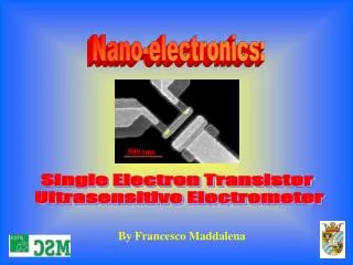
Nano-electronics
Nano-electronics. Vision: Instrumentation and methods for analysis of atomic scale physical properties, and methods to correlate these properties with nano-electronic device and system performance. Nano-electronics: hard problems.

Nano-electronics
E N D
Presentation Transcript
Nano-electronics • Vision: Instrumentation and methods for analysis of atomic scale physical properties, and methods to correlate these properties with nano-electronic device and system performance.
Nano-electronics: hard problems • Spatially resolved characterization (1-, 2-, and 3-D as appropriate) of physical properties, ranging from nanometer to atomic scale: • Physical properties of interest include chemical composition, electrical, thermal, structural, mechanical and optical properties. • Hierarchical multiscale modeling methods to correlate measured physical properties with device electrical properties. • Standardized methods/models for analysis of metrology data. • For manufacturing these metrologies should be: • Statistically significant and determine nano-property distribution over the chip, across the wafer, and wafer to wafer. • Compatible with the high-throughput, high-sensitivity, non-destructive, and low-cost, environment of semiconductor manufacturing
Industrial sectors with significant R&D and products in nanotechnology • Telecommunications • Chemicals/catalysis • Homeland security • Transportation • Life Sciences • Electronics • Coatings • Defense • Sensors • Energy
Nanophotonics Grand Challenge Vision (I) • Vision: • Design, model, and synthesize materials and devices for optoelectronics,data storage, efficient light sources, optical computing, and biomedical instrumentation • Develop instrumentation and techniques for nanoscale 3D imaging, chemical analysis, and material manipulation in hard and soft materials • Hard Problems: • Interface control in heterogeneous materials synthesis • Integration of device and materials with different properties and functionalities • Challenges in sub-surface and 3D imaging from nano to meso scale • New components and devices that improve signal, speed, and resolution by orders of magnitude • Realistic 4D modeling of entire optical systems below the diffraction limit • Precision measurements of materials optical properties over wide range of conditions
Nanophotonics Grand Challenge Vision (II) • Industrial benefits: • High throughput, high yield nano-manufacturing • New methods in optical communications • Bio-medical in-vivo sensors and diagnosis • Low-cost, long-duration light sources and detectors • General public impacts: • High-security, low-power, high-speed communications • New bio-medical knowledge enabling acceleration of drug discoveries • New photodynamic therapies • Homeland security: sensors for bio/chemical detection
Nanomagnetics Grand Challenges • Measurement of magnetic properties of one cn (cubic nm) of material. • Imaging of spin dynamics at the nano-scale with sub-ns time resolution • Measurement of spin transport in materials (e.g. semiconductors)
Measurement of magnetic properties of one “cn” (cubic nm) of material. • Measure 10-17 emu (100 atoms) • Measure inter- particle & inter–grain magnetic interaction with spatial resolution <1 nm • Exchange and magneto-static interactions • Probe buried interfaces • Probe structural and electronic properties of tunnel barriers • Image magnetic polarization of 1 cn of material
Imaging of spin dynamics at the nano-scale with sub-ns time resolution • 3D magnetization measurements • Element specificity at < 10 nm resolution • Gives resolution better than exchange length • Accurate modeling of selected probe techniques to analyze and direct research. • Develop x-ray optics for photoemission, diffraction, and dichroism experiments
Measurement of spin transport in materials • Develop Tools to measure spatial dependence of spin polarization in materials • Interfaces and nanostructured materials and bulk • Develop Tools to measure spin transport and accumulation • Optical methods to generate and manipulate spin currents • Modeling to infer spin polarization
Applications • Magnetic recording: density increased beyond 10 Tb/cm2 • Permanent magnets: 4pM>2 kA/m • Magnetic-RAM: in production • Nonvolatile, high speed, low power, • “instant on” computers • Improved field sensors: • Applications in military, biomedical, security
Combined Grand Challenge • Develop instrumentation and methods for the measurement & analysis of atomic scale (1 cn) electronic, photonic, and magnetic properties, and methods to correlate these properties with nano-materials, devices and system performance.