NANO ELECTRONICS TECHNOLOGY
210 likes | 698 Vues
MANISH GUPTA. NANO ELECTRONICS TECHNOLOGY. Presentation Outline. Introduction Motivation Content Expected Impact Funding Schemes & Budget. Introduction: Main Principles. Continuity: Same structure of challenges and objectives as in WP 07-08 2 years duration Adaptation:

NANO ELECTRONICS TECHNOLOGY
E N D
Presentation Transcript
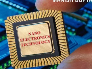
MANISH GUPTA NANO ELECTRONICS TECHNOLOGY
Presentation Outline • Introduction • Motivation • Content • Expected Impact • Funding Schemes & Budget
Introduction: Main Principles • Continuity: • Same structure of challenges and objectives as in WP 07-08 • 2 years duration • Adaptation: • Within Challenges, objectives to be adapted to technological evolutions, socio-economic developments and lessons from first calls • Existing objectives to be reworked, replaced or removed • Complementarity with JTIs and Art.169 initiative
Introduction: • A WP structured around a limited set of “Challenges” that should be addressed • A Challenge is • Focusedonconcrete goals that require effort at Community level and where collaboration is needed • Ambitious and strategicproposing a European vision on ICT for the next 10 to 15 years • Described in terms of the set of outcomes targeted and their expected impact on industrial competitiveness and on addressing policy and socio-economic goals
Digital libraries & content Chal-4 Sustainable & personalised healthcare Chal-5 Mobility, environment. sustain. and energy efficiency Chal-6 Indep. living inclusion & participatorygovernance Chal-7 Pervasive &Chal-1 trustworthy network and servic. infrast. Cognitive systems, robotics and interaction,Chal-2 Electronics components and systems Chal-3 Introduction: ICT Work Programme 2009-10 End-to-end Systems, Socio-economic Goals Call 4:19 Nov 08 - 1 April 09 801 M€ Call 5:31 July 09 – 3 Nov 09722 M€ Call 6:24 Nov 09 – 13 April 10 286 M€ Future and Emerging ICT Technology Roadblocks
Technology-led challenges removing roadblocks and improving the capability of generic technology components, systems and infrastructure Application-led challenges new technology-based systems, products and services that provide step-changes in the capabilities of the resulting solution Synergies throughout the Programme The ICT WP addresses a research problem through different angles corresponding to different technological challenges
Components, Systems, Engineering Objectives • IST-2007.3.2:Design of semiconductor components and electronic-based miniaturised systems (25 M€) • IST-2007.3.3:Flexible organic and large area electronics (60 M€) • IST-2007.3.4:Embedded systems design (28 M€) • IST-2007.3.6:Computing systems (25 M€) • IST-2007.3.8:Organic photonics and other disruptive photonics technologies (30 M€) • IST-2007.3.1:Nanoelectronics technology (35 M€) • IST-2007.3.5:Engineering of networked monitoring and control systems (32 M€) • IST-2007.3.7: Photonics(60 M€) • IST-2007.3.9: Microsystems and smart miniaturised systems (80 M€) Call 4 Nov 2008 Call 5 July 2009
European Roadmap for Nanoelectronics More than Moore: Diversification Analog/RF Passives HV Power SensorsActuators Biochips Interacting with people and environment Non-digital content SoC & System-in-Package (SiP) 130nm 90nm Moore’s Law: Miniaturization 65nm Combining SoC and SiP: Higher Value Systems Information Processing Digital content System-on-Chip (SoC) Baseline CMOS: CPU, Memory, Logic 45nm 32nm 22nm Beyond CMOS
Nanoelectronics in Framework • WP 2007-2008:Next-Generation Nanoelectronics Components & Electronics Integration (call1 86 M€) • Smaller, higher performance, lower cost: “More Moore” • Integration and diversification: Systems-on-Chip, Systems-in-Package • Long Term Future: Beyond CMOS • (Technology - Design - Manufacturing – Equipment) WP 2009-2010:Nanoelectronics Technology and Manufacturing (call 5 – 35 M€) WP 2009-2010:Design of semiconductor components and electronics based miniaturised systems (call 4 – 25 M€)
Thematic Coverage Technology Requested: 137 M€ Funded:50 M€ 37 % Design Requested: 108 M€ Funded:9 M€ 8 % Modelling Requested: 17 M€ Funded:5 M€ 29 % Generic Requested: 12 M€ Funded:6 M€ 50 % Equipm./Metrol. Requested: 79 M€ Funded:12 M€ 15 % Manufacturing Requested: 28 M€ Funded:5 M€ 18 %
The continuous miniaturisation on integrated electronic components has almost reached the physical and technological limits • integration of a large number of less known materials • complex technological solutions • increase of R&D and semiconductor manufacturing costs Industrial R&D in Europe is shifting towards a product oriented approach by adding extra functionalities to the basic components Motivation Combination of miniaturisation and functionalisation, ‘More Moore’ and ‘More than Moore’ devices into total system solutions through the process of monolithic and heterogeneous integration
Motivation • Challenges Manufacturing: • Reduce cycle time • Enhance production quality and variability control • Improve equipment productivity • Reduce the environmental impact • Support heterogeneous integration • Foster advanced system integration and functionalized packaging
Objective: Nanoelectronics technology Focus on: • Miniaturisation and functionalisation • Beyond CMOS domain • Advanced aspects of the ‘More than Moore’ domain • their integration and their interfacing with existing technologies • Manufacturing technologies • Flexible manufacturing with a high product mix and joint equipment assessment • prepare for more disruptive approaches • Support measures
Target outcome • Miniaturisation and functionalisation • Beyond 22 nm devices, advanced components with lower scaling factors including non-CMOS devices, and • their integration and interfacing with very advanced CMOS Activities with a high risk factor Industrialisation perspective beyond 2014 and having a generic development focus Funding schemes: STREPs NoE
Target outcome • Manufacturing technologies • New semiconductor manufacturing approaches, processes and tools • Joint assessments of novel process/metrology equipment and materials • Supporting 200/300mm wafer integration platforms • Preparatory work for 450mm wafer processing Funding schemes: STREPs IP
Target outcome • Support measures • Roadmaps, benchmarks, selection criteria for the industrial use of ‘Beyond CMOS’ • Access to affordable silicon state-of-the-art technologies for prototyping and low volume and to design expertise and commercial tools • Stimulation of interest of young people, training and education • Linking of R&D strategies and stimulation of International Cooperation • Support and coordination of preparatory work for 450 mm processing and equipment Funding schemes: CSA Budget: 4.5 M€
Expected Impact • Strengthened competitiveness of the European nanoelectronics industry • Contribution to the competitiveness and the attractiveness of Europe to investments • New electronics applications of high economic and socio-economic relevance • Maintained European knowledge and skills, • Increased critical mass of resources and knowledge, • Contribution to preserving a critical mass of manufacturing capacity in Europe
