Analog FE Circuitry Simulation for ECAL/HCAL Electronics Upgrade
60 likes | 173 Vues
PSPICE simulation of the FE analog part for ECAL/HCAL electronics with real signals, cables, amplifiers, and more. Detailed analysis with recommendations for better performance and cost estimates.

Analog FE Circuitry Simulation for ECAL/HCAL Electronics Upgrade
E N D
Presentation Transcript
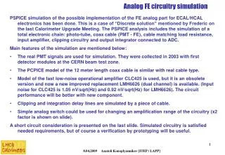
Analog FE circuitry simulation • PSPICE simulation of the possible implementation of the FE analog part for ECAL/HCAL electronics has been done. This is a case of “Discrete solution” mentioned by Frederic on the last Calorimeter Upgrade Meeting. The PSPICE analysis includes the simulation of a total electronic chain: photo-tube, coax cable (PMT - FE), cable matching load resistance, input amplifier, clipping circuitry and output integrator connected to ADC. • Main features of the simulation are mentioned below: • The real PMT signals are used for simulation. They were collected in 2003 with first detector modules at the CERN beam test zone. • The PCPICE model of the 12 meter length coax cable is similar with real cable type. • Model of the fast low-noise operational amplifier CLC425 is used, but it is an obsolete version and now a new improved replacement LMH6626 (dual channel) is available. (Input noise for CLC425 is 1.05 nV/sqrt(Hz) and 0.92 nV/sqrt(Hz) for LMH6626). The circuit performance will be better with new component. • Clipping and integration delay lines are simulated by a piece of cable. • Simple analog switch could be used for changing an amplification range of the circuitry (x2 factor is shown on slide). • A short circuit consideration is presented on the last slide. Simulated circuitry is satisfied needed requirements, but of course a verification by prototyping will be useful. 8.04.2009 Anatoli Konoplyannikov [ITEP / LAPP]
Analog FE circuitry simulation HCAL signal shapes on 80 GeV electron response. (1 – non clipped; 2 – clipped signal) HCAL signal shapes on 50 GeV pion response. (non clipped signal) Applied for simulation signal shapes were obtained (recorded by scope) during the HCAL/ECAL modules test beam study in 2003. 8.04.2009 Anatoli Konoplyannikov [ITEP / LAPP]
Analog FE circuitry simulation Input ADC Simulated circuitry of the analog chain of the FE electronics. 8.04.2009 Anatoli Konoplyannikov [ITEP / LAPP]
Analog FE circuitry simulation Flat top Residual level Integrator-shaper output response on 50 pC PMT signal charge. The integrator signal “flat top” is about 3 ns and residual level less than 1 %. 8.04.2009 Anatoli Konoplyannikov [ITEP / LAPP]
Analog FE circuitry simulation Spectral current noise at the input (on PMT anode) Spectral voltage noise at the output Total noise voltage at the output Noise characteristics of the analog circuitry. Total output voltage noise is less than 0.4 mV. (about 1.2 counts for a 12 bit ADC with input range of about 1300 mV) 8.04.2009 Anatoli Konoplyannikov [ITEP / LAPP]
Analog FE circuitry simulation • Circuit consideration • OA LMH6626 main characteristics: • Gain bandwidth (LMH6624) 1.5GHz; • Input voltage noise 0.92nV/sqrt(Hz); • Input offset voltage (limit over temp) 700uV • Supply voltage range (dual supply) ±2.5V to ±6V • Room on the PCB: • The LMH6626 is offered in SOIC-8 and MSOP-8 packages. Dimension of SOIC-8 is 5 mm x 6 mm. Two packages of OA per FE channel take small room. More room will be needed for two delay lines. In my opinion, the needed room on the FE board is less or the same as on the existing FE board. • Power consumption: • Supply current for each OA is 12 mA. In total about 50 mA per a FE channel will be needed and about 1.6 A per 32 channel board. • Price estimation: • Each front-end channel will be equipped with two LMH6626 chips (price for one chip is $ 2.05), two delay lines 10 ns and 25 ns (the type of the delay line could be as for the present FE boards), resistors and capacitors. Total component price per channel will be about $ 10 (in case if delay line price is about $ 2). 8.04.2009 Anatoli Konoplyannikov [ITEP / LAPP]
