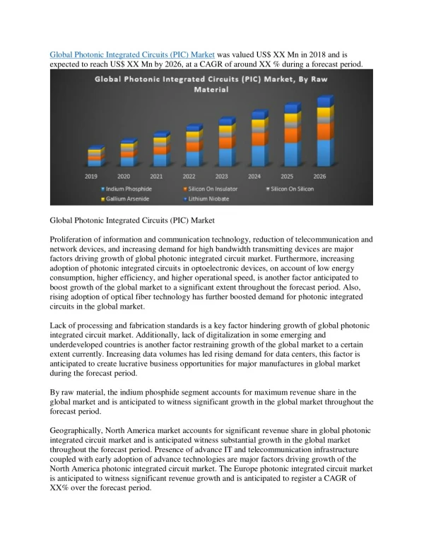
Download
1 / 12
340 likes | 1.08k Vues
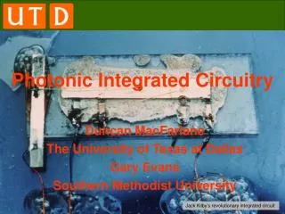
Photonic Integrated Circuitry. Duncan MacFarlane The University of Texas at Dallas Gary Evans Southern Methodist University. Jack Kilby’s revolutionary integrated circuit. Introduction. Early electronic filters used only L, C and R’s – “Passive Filters”

E N D
Photonic Integrated Circuitry Duncan MacFarlane The University of Texas at Dallas Gary Evans Southern Methodist University Jack Kilby’s revolutionary integrated circuit
Introduction • Early electronic filters used only L, C and R’s – “Passive Filters” • Gain elements, first vacuum tubes, later transistors, allowed “Active Filters” • Current optical filters are purely passive • It is time to develop optical filters with gain that are higher performance, and adaptive We are developing a manufacturable, programmable, Photonic Integrated Circuit!
G G tk-1 Tk(z) tk Tk+1(z) Z-1/2 + + rk-1 -rk-1 rk -rk Rk(z) Rk+1(z) Z-1/2 + + tk-1 tk Active Lattice Filters An active optical filter has a gain element that allows the weights associated with the different poles and zeroes to be tuned. • Gain allows: • Improved quality factors • Adaptive filters • Lattice Filters good for: • Linear Prediction • Frequency Discrimination • Robust wrt realization limitations Gain Block Delay Block
Surface Grating Photonic IC We are using the GSE technology for integrated active optical filters Grating Gain Region
Four Directional Couplers • Grating can couple in multiple directions • Input/output • Mesh structure • FIB nanostructure • Holographic lithography • Two step process • Crossed Gratings
Two Dimensional GSE Lattices Completely new filter structure solved by layer peeling with 2nx2n matrices … Research is benefiting fundamental DSP engineering ~60 um
Two Dimensional GSE Lattices • Multiple Input, Multiple Output Applications • Add/drop applications, dwdm, o-cdma on same chip • Cross correlators, decouplers, cross-talk cancelation • multi-trajectory tracking, joint process estimation • Fully Tunable … programmable • Extends the palette of filter realizations for optimal implementations
Frequency Selection Stable operation with Q >75,000
Economically Viable Device • Structure is highly manufacturable • Standard Epitaxy • Photolithographic gratings • Last step in process • No regrowth • Chip scale process (parallel) • Being commercialized for lasers • Basic structure can be standardized for fabrication purposes • Individual users may then program them for a particular application • Just like an FPGA or a DSP
Outcome of the Research Program • Standardized Photonics • Two dimensional lattice has wealth of transfer functions supporting widespread applications • Programming determines application • Basic advances in DSP • Two dimensional structure is new • Highly appropriate for MIMO applications 100 GHz clock rates and GHz tuning rates will enable high volume information engineering applications