Download

1 / 3
40 likes | 192 Vues
This article explores an innovative technique for inspecting solder shapes on PCB boards using an intelligent digital satellite receiver system. By employing a structured highlight method and multiple point sources, it effectively illuminates and images specular surfaces to extract three-dimensional shape information. The approach involves capturing the reflected highlight patterns and using geometric relations to determine the orientation of surface elements and solder height. This method yields depth maps and reconstructed solder shapes for enhanced quality control in electronics manufacturing.

E N D
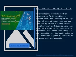
PCB Soldering Inspection Intelligent Digital Satellite Receiver System
Normal vector at high Lighted point (i,j) is Structured Highlight method is applied to illuminating and imaging specular surfaces which yields three dimensional shape information This approach uses multiple point sources and images the resulting highlight patterns reflected from the surface Assumption: Then: Solder Shape Using total K images Vector field is given: • A fixed camera images the reflected light ray only if it is positioned and oriented such that it is admitted by the camera’s projective axis • Once the reflected light ray is observed as a highlight in the camera image and the direction of incident ray is known, orientation of the surface element where light was reflected can be found Structured Highlight approach Solder Height Detection Basic Geometric Relations These can be rewritten as:
Full Depth Map Selected Area Experimental Setup Simulated Results Board Image • Processing • Find Normal vector • Vector Field • Solder Height • Depth Map Sample PCB board images Reconstructed Solder Shape