Download

1 / 11
160 likes | 593 Vues
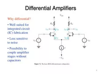
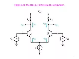
BJT Differential Pair. Transistors Q1, Q2 are matched Responds to differential mode signals. (a) The differential pair with a common-mode input signal v CM . (b) The differential pair with a “large” differential input signal. . 6-1. BJT Differential Pair. (d). (c).

E N D
BJT Differential Pair Transistors Q1, Q2 are matched Responds to differential mode signals (a) The differential pair with a common-mode input signal vCM. (b) The differential pair with a “large” differential input signal. 6-1
BJT Differential Pair (d) (c) (c) The differential pair with a large input signal of polarity opposite to that in (b). (d) The differential pair with a small differential input signal vi. 6-2
BJT Differential Pair Small-Signal Operation 6-4
Differential Voltage Gain Vd less DC DC Differential output Single-ended output Differential output with emitter Resistance RE 6-5
Differential Half-Circuit vC2 = -vC1 voltage gain = gain of ½ cct (output taken differentially) Fig. 6.7 Equivalence of the differential amplifier (a) to the two common-emitter amplifiers in (b). This equivalence applies only for differential input signals (unless R >> re). Either of the two common-emitter amplifiers in (b) can be used to evaluate the differential gain, input differential resistance, frequency response, and so on, of the differential amplifier (e.g. using hybrid pi model). 6-6
Common-Mode Gain Analyzing the equiv. Circuit (b) For output taken differentially = 0 and common-mode gain = 0 For output taken single-ended 6-7
Common-Mode Gain (Cont’d) Consider the case of a collector resistor mismatch Q1 has load Q2 has load (differential component) (common-mode component) (P) 6-8
Input Common-Mode Resistance Input CM resistance is large so we must take into account CM gain is small, so assume 0V at collector then r0 appears in parallel with 2R in the emitter and ru appears between input and ground. “emitter reflectance rule” 6-9 (P)
Example6.1 pg. 502 15V 10k 10k - vo+ vs 150 150 1mA 200k 6-10 (P)
Example6.1 pg. 502 (Cont’d) (c) The worst case common-mode gain if the two collector resistances are accurate to within 1% where DRC = 0.02 RC (worst case) (d) The CMRR in dB Using Ad = 40 from (b) and ACM = 5E-4 from ( c) (e) The input common mode resistance (assuming VA = 100 and rm = 10 br0) Eqn. 6.44 p 502