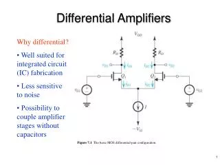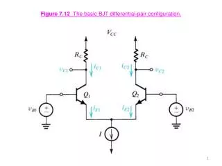
Figure 7.12 The basic BJT differential-pair configuration.
350 likes | 977 Vues
Figure 7.12 The basic BJT differential-pair configuration. Figure 7.13 Different modes of operation of the BJT differential pair: (a) The differential pair with a common-mode input signal v CM . .

Figure 7.12 The basic BJT differential-pair configuration.
E N D
Presentation Transcript
Figure 7.13 Different modes of operation of the BJT differential pair: (a) The differential pair with a common-mode input signal vCM.
Figure 7.13 Different modes of operation of the BJT differential pair: The differential pair with a “large” differential input signal.
Figure 7.13 The differential pair with a large differential input signal of polarity opposite to that in (b).
Figure 7.13 The differential pair with a small differential input signal vi. Note that we have assumed the bias current source I to be ideal (i.e., it has an infinite output resistance) and thus I remains constant with the change in vCM.
Figure 7.14 Transfer characteristics of the BJT differential pair of Fig. 7.12 assuming a= 1.
Figure 7.6 Normalized plots of the currents in a MOSFET differential pair. Note that VOVis the overdrive voltage at which Q1 and Q2 operate when conducting drain currents equal to I/2.
Figure 7.15 The transfer characteristics of the BJT differential pair The linear range of operation can be extended by including resistances in the emitters.
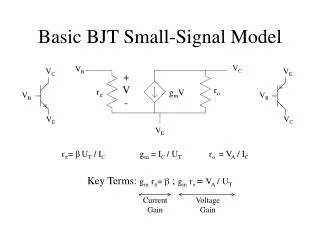
Figure 7.16 The currents and voltages in the differential amplifier when a small differential input signal vid is applied.
Figure 7.17 A simple technique for determining the signal currents in a differential amplifier excited by a differential voltage signal vid; dc quantities are not shown.
Figure 7.18 A differential amplifier with emitter resistances. Only signal quantities are shown (in color).
Figure 7.19 Equivalence of the BJT differential amplifier : Two common-emitter amplifiers
Figure 7.20 The differential amplifier fed in a single-ended fashion.
Figure 7.19 Equivalence of the BJT differential amplifier : Two common-emitter amplifiers
Figure 7.4 The MOS differential pair with a differential input signal vidapplied.
Figure 7.20 The differential amplifier fed in a single-ended fashion.
Figure 7.21 The differential half-circuit and its equivalent circuit model
Figure 7.22 The differential amplifier fed by a common-mode voltage signal vicm.
Figure 7.23(a) Definition of the input common-mode resistance Ricm. (b) The equivalent common-mode half-circuit.