First Time User Guide to PN Junction V1.31
160 likes | 393 Vues
First Time User Guide to PN Junction V1.31. Saumitra R Mehrotra*, Ben Haley & Gerhard Klimeck Network for Computational Nanotechnology (NCN) Electrical and Computer Engineering http://nanohub.org/resources/229 *smehrotr@purdue.edu. Outline. Introduction What is a PN Junction?

First Time User Guide to PN Junction V1.31
E N D
Presentation Transcript
First Time User Guide toPN Junction V1.31 Saumitra R Mehrotra*, Ben Haley & Gerhard Klimeck Network for Computational Nanotechnology (NCN) Electrical and Computer Engineering http://nanohub.org/resources/229 *smehrotr@purdue.edu
Outline • Introduction • What is a PN Junction? • Working of a PN Junction. • What can be simulated by in PN Junction Lab? • What if you just hit “Simulate”? • Examples • What if the doping is changed? • What if the intrinsic region is included (e.g. PIN diode)? • Limitation/Comments • References
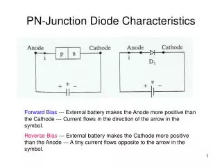
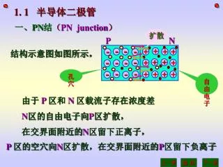
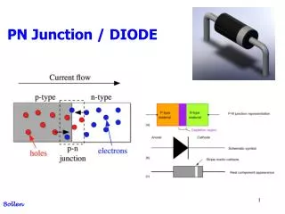
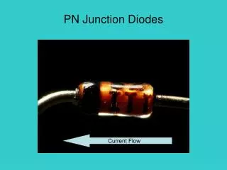
What is a PN Junction? • A PN junction is a device formed by combining p-type ( doped with B,Al) and n-type (doped with P,As,Sb) semiconductors together in close contact. • PN junction can basically work in two modes, • forward bias mode (as shown below: positive terminal connected to p-region and negative terminal connected to n region) • reverse bias mode ( negative terminal connected to p-region and positive terminal connected to n region) PN junction device
Working of a PN junction Current I-V characteristic of a PN junction diode. Reverse Bias Forward Bias Zener or Avalanche Breakdown Voltage • PN junction diode acts as a rectifier as seen in the IV characteristic. • Certain current flows in forward bias mode. • Negligible current flows in reverse bias mode until zener or avalanche breakdown happens. Refer https://nanohub.org/resources/68 for a detailed discussion on operation of PN junction.
What can be simulated in PN junction lab? PN junction device structure Specify P-type region length. (More number of nodes lead to higher resolution but also more compute time) Specify intrinsic region length Specify N-type region length Specify doping level for P-type and N-type region.
What can be simulated in PN junction lab? PN junction material definition Specify the material to be simulated (Si,Ge,GaAs) Specify intrinsic minority carrier lifetime (s).
What can be simulated in PN junction lab? PN junction environment definition Specify temperature (K). Specify applied voltage and number of steps.
What can be simulated in PN junction lab? PN junction output plots Default settings will simulate : PN junction diode in forward bias mode with, 1m long P-type and N-type regions doped at 1e17 cm3.
What if you just hit simulate? • IV characteristic for PN junction in forward bias mode in default settings. • Current increases slightly till Knee Voltage*. • Beyond it current rises exponentially. Knee voltage *Refer https://nanohub.org/resources/68 for a detailed discussion on operation of PN junction.
What if you just hit simulate? • C d –1[1]&[2] where, C : capacitance across PN junction & d : depletion width* (insulating region at the junction where carriers have diffused away or have been swept by the electric field.) • Increasing bias decreasing depletion width Increasing Capacitance C-V characteristic for PN junction in forward bias mode in default settings. *Refer https://nanohub.org/resources/68 for a detailed discussion on operation of PN junction.
What if you just hit simulate? Built in charge, electric field and potential at equilibrium. P-region N-region Built in charge Built in potential, Vbi= 0.834V P-region N-region Built in electric field
What if you just hit simulate? Built in charge, electric field and potential at forward bias Va=0.6V P-region N-region Potential difference Vbi-Va= 0.234V Decreasing charge with applied bias due to thinning of depletion width. Increased diffusion of electrons across the barrier lowered by Va. Positive bias at P side reduces the barrier leading to increase in diode current. P-region N-region Decreasing electric field with applied bias due to thinning of depletion width.
What if doping is changed? On changing doping for both n-type and p-type regions from 1e16 cm3 to 1e18 cm3. • Increasing doping leads to increasing built in potential, Vbi [1],[2]. • Na : P region doping level (cm-3). • Nd : N region doping level (cm-3). • ni : Intrinsic carrier density (cm-3). • KbT : Thermal voltage (= 0.0259 V). Doping= 1e18 cm3 = Vbi Doping= 1e16 cm3
What if intrinsic region is included i.e PIN diode? On introducing an intrinsic region of length 0.2 m with default setting. PIN diode (bold) PN diode (light) Increased depletion width (d) due to addition of intrinsic region as seen in energy band diagram. Junction Capacitance, Cj d-1 shows a decrease as seen in CV characteristic.
Limitations/Comments • Large physical dimensions (>10um) might lead to non convergence or large compute time. • More nodes might be required for better convergence in some cases i.e. high doping in PN junction. • PN junction currently performs steady state simulations only, no time dependent simulations are possible. • Contacts during the simulation are considered to be ohmic (i.e. Current-Voltage,I-V curve is linear and symmetric).
References • PN junction theory • [1] PN junction OPERATION : https://nanohub.org/resources/68 • [2] “Semiconductor Device Fundamentals”, by R.F. Pierret • PADRE • [3] Dragica Vasileska; Gerhard Klimeck (2006), "Padre," DOI: 10254/ nanohub-r941.3. • [4] PADRE MANUAL : http://nanohub.org/resource_files/tools/padre/doc/ index.html • Please report any comment/review at the following link, • https://nanohub.org/resources/pntoy/reviews • If you reference this work in a publication, please cite as follows: • Matteo Mannino; Dragica Vasileska; Michael McLennan; Xufeng Wang; Gerhard Klimeck (2005), "PN Junction Lab," DOI: 10254/nanohub-r229.9.