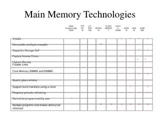
Main Memory
Main Memory. Computer Science & Engineering Department Arizona State University Tempe, AZ 85287 Dr. Yann-Hang Lee yhlee@asu.edu (480) 727-7507. Memory Technology. “Non-so-random” Access Technology: Access time varies from location to location and from time to time

Main Memory
E N D
Presentation Transcript
Main Memory Computer Science & Engineering DepartmentArizona State University Tempe, AZ 85287 Dr. Yann-Hang Leeyhlee@asu.edu(480) 727-7507
Memory Technology • “Non-so-random” Access Technology: • Access time varies from location to location and from time to time • Examples: Disk, tape drive, CDROM • Random Access: Mem(address) data • “Random” is good: access time is the same for all locations • DRAM: Dynamic Random Access Memory • one transistor per cell • High density, low power, cheap, slow • Dynamic: need to be “refreshed” regularly • SRAM: Static Random Access Memory • 4-6 transistors per cell • Low density, high power, expensive, fast • Static: content will last “forever”
Wr Driver Wr Driver Wr Driver Wr Driver - + - + - + - + A0 A1 A2 A3 - + - + - + - + Sense Amp Sense Amp Sense Amp Sense Amp A 16X4 SRAM Din 3 Din 2 Din 1 Din 0 WrEn Precharge Word 0 SRAM Cell SRAM Cell SRAM Cell SRAM Cell Word 1 Address Decoder SRAM Cell SRAM Cell SRAM Cell SRAM Cell : : : : Word 15 SRAM Cell SRAM Cell SRAM Cell SRAM Cell Dout 3 Dout 2 Dout 1 Dout 0
SRAM Cell Architecture • Write: • Drive bit lines (bit=1, bit=0) • Select row • Read: • Precharge C and C to Vdd • Select row • Cell pulls one line low • Sense amp on column detects difference between C and C
SRAM Read Operation • read cycle time -- trc • address access time – taa • CS to access time – tacs • OE to output valid -- toe
SRAM Write Operation • write cycle time – twc • end of write • write pluse width -- twp
DRAM • A grid of capacitors to hold data bits • To access a bit • row address strobe (RAS) – to transfer an entire row to sense amplifier • column address strobe (CAS) – to choose a specific cell • refresh – to recharge the capacitors • Every time a row is read and also done periodically • Example: 2 Mb DRAM = 256K * 8 = 512 rows * 512 cols * 8 bits cell array N bits 512 cols 512 Plane 7 r o w 512 256 Kb DRAM 512 rows Plane 1 addr Plane 0 c o l 256 Kb DRAM D<7> One “Plane” of 256 Kb DRAM sense D<1> D<0> D
Cycle Time Access Time Memory Bank 0 bank 0 Memory Bank 1 bank 1 CPU Memory Bank 2 bank 2 1st read 2nd read Memory Bank 3 3rd read DRAM • 1-transistor cell: data is stored in a capacitor • Read: read and recharge • Refresh: a dummy read to recharge the capacitor • DRAM (Read/Write) Cycle Time >> DRAM (Read/Write) Access Time • Interleaving:
Different DRAMs • Asynchronous DRAM • FPM (fast page mode) • for each RAS, consecutive CAS to access bits in the same row • EDO (extended data out) • overlap data output and the next CAS (pipelined) • SDRAM (synchronous) • interleaved (2 banks)– one is refreshing and the other can be accessed • synchronized to clock and burst mode (without CAS) • Example: Micron SDRAM (MT48LC1M16A1) • dual 512K*16 DRAM – 2048 rows by 256 columns • burst access with lengths 1, 2, 4, 8, and full page • auto precharge function – self-timed row precharge at the end of the burst sequence • auto refresh -- internal refresh counter for row addresses • tref= 64ms (2048 auto refresh cycles every 64ms), i.e. once every 31.25s
Micron MT48LC1M16A1 Block Diagram • CLK, CKE (clock enable) • CS# (chip select) • WE# (write enable), RAS#, CAS# • BA (bank address) • A0-A10 (address) • DQ0-DQ15 (data I/O) • DQML,DQMH (input/output mask) – mask low or high bytes when write or enable output when read
SDRAM Read Operation • SDRAM has been initiated and mode register is loaded • Active (RAS) and then Read (with A10 high for auto precharge) • CAS latency: delay between read command and the availability of the 1st piece of output data • CL2 or CL3: 2 or 3 clock cycles • Timing parameters: • tRCD: between Active and Read/Write (RAS and CAS) • tRAS : between Active to Precharge • tRC : between successive Active’s to the same bank • tRRD : between successive Active’s to different banks
DDR (Double Data Rate) SDRAM • Same memory core • identical addressing and command control, refresh requirements • different data interface • At a data rate twice of the clock frequency • The internal bus is twice of the width of the external bus • data capture at both edges • Source-synchronous interfaces:
DDR Read Operation • DQS: data strobe • bi-directional, by the controller for write and DRAM for read • Either one of the two words read can be ignored. • DQS is edge aligned with DQ (clocked out at the same internal signal
DDR Write Operation • DQS is center-aligned relative to DQ and is used to capture input data
DIMM • 184-pin dual in-line memory module (DIMM) • 128MB (16 Meg x 64), 256MB (32 Meg x 64), or 512MB (64 Meg x 64) • ECC (-- x 72) • 8 or 4 DRAM chips • Serial presence-detect (SPD) – a 256 bytes EEPROM • to identify the module type and various SDRAM organizations and timing parameters • I2C interface with the controller • Registered– for servers, router, etc. • To assure data integrity, use registers to latch address and command signals and one PLL clock buffer to adjust timing. • Unbuffered -- cost optimized for desktop PC • 200-pin, small outline, dual in-line memory module (SODIMM)
SDRAM Configuration Example • Assume we have 4 MT48LC32M8A2 chips • each one is with 8 Meg x 8 x 4 banks (256M bits) • need 4 chips to make a memory of 32-bit data • Addresses (10+2+13=25 bits) • banks: BA0-BA1 (2) • Row: A0-A12 (13) • Column: A0-A9 (10) • CPU sends 32-bit addresses • AD0-AD1 to select a byte from a word • AD2-AD11, i.e. column address, to select a word from a row • AD12-AD24 as row address • AD25-26 connected to BA0-BA1 (non-interleaved) • AD27-31 to select the SDRAM memory (to enable CS)
SDRAM Configuration Example • Assume CPU reads • one word from memory location 0x09050120 • CS=0x01, Row=0x1050, Bank=0b00, Column=0x044 • two words from memory location 0x09050184 • CS=0x01, row=0x1050, Bank=0b00, Column=0x061 • Burst length=1, tRCD =1.6 clock periods, and CAS Latency=2