ECE122 – 30 Lab 3: Layout of a Buffer
200 likes | 391 Vues
The George Washington University School of Engineering and Applied Science Department of Electrical and Computer Engineering. ECE122 – 30 Lab 3: Layout of a Buffer. Jason Woytowich Ritu Bajpai September 22, 2005. Layout Using L-Edit. Create a module of a buffer, using SCMOS inverters

ECE122 – 30 Lab 3: Layout of a Buffer
E N D
Presentation Transcript
The George Washington UniversitySchool of Engineering and Applied ScienceDepartment of Electrical and Computer Engineering ECE122 – 30 Lab 3: Layout of a Buffer Jason Woytowich Ritu Bajpai September 22, 2005
Layout Using L-Edit • Create a module of a buffer, using SCMOS inverters • Don’t forget to make a symbol for it
Layout Using L-Edit • Instance your buffer into a new module and add pads to the inputs and outputs. • I called it Buffer_wPads
Layout Using L-Edit • Export your design as a tpr file.
Layout Using L-Edit • Open L-Edit • Replace Setup: C:\TannerLib\SCMOS\mhp_n05d.tpr
Layout Using L-Edit • Go to SPR->Setup • Fill in the paths for the tech library and your netlist
Layout Using L-Edit • Go to SPR->Place and Route, Hit Run
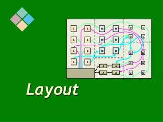
Layout Using L-Edit • If it completes correctly you will see this:
Layout Using L-Edit • Cross sections • Process Definition File is C:\Program Files\Tanner EDA\L-Edit 11.0\samples\tech\mosis\mhp_n05.xst
Simulating Your Layout • Once the we have a layout we can simulate our design with parasitic capacitances. • First draw ports over each of the pad with Metal3 selected. • Give them descriptive names
Simulating Your Layout • Copy the file C:\TannerLib\tech\mosis\mhp_n05.ext into your working directory • Make the following modification # Linear capacitor using Cap-Well # device = CAP( # RLAYER=cap using Cap-Well; # Plus=poly wire; # Minus=ndiff; # MODEL=; # )
Simulating Your Layout • Go to Tools->Extract
Simulating Your Layout • Open the output in T-Spice • Add simulation commands and power supplies • Replace signal names where necessary .include "C:\Program Files\Tanner EDA\T-Spice 9.1\models\ml2_125.md" .tran/powerup 2n 400n method=bdf .print tran v(Pad_Input,Ext_Gnd) v(Pad_Output,Ext_Gnd) V1 Ext_Vdd Ext_Gnd 5.0 V2 Pad_Input Ext_Gnd PULSE (5V 0V 0 1n 1n 50n 100n)
Homework • Implement the following functions as a single module using only NAND gates from the SCMOS library. • Test and layout. • Extra points for optimal designs X = ((!A)B + A(!B)C)