RF Troubleshooting Training Course
Learn to troubleshoot RF systems including receiver and transmitter flow charts. Understand GSM and DCS frequencies. Hands-on practice with RF instruments.

RF Troubleshooting Training Course
E N D
Presentation Transcript
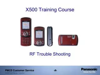
X500 Training Course RF Trouble Shooting
RF & TX Part RF & Transmitter Field
Rx Receiver Flow Chart U503 F501&F502 U501
Receiver Flow Chart Rx :Set RF Measure Instrument: HP8960 or HP8922 • 1. Operating mode Test mode , Test function TW • 900/1800 Bend: • Ch 62 947.4MHz , Cell power -60dBm (Ch699: 1842.6MHz) • 3 850/1900 Band: • Ch 189 881.4MHz , Cell power -60dBm (Ch661: 1.96GHz)
Receiver Flow Chart Step 1. Check JP1 first, if we don’t insert RF cable, pin 1 must short to pin 2 Step 2. Use probe, touch C540 pin 1 : ~ -61dBm GSM Freq = 947.4MHz DCS Freq = 1842.6MHz S2 S1
Receiver Flow Chart Step 3. Use probe to touch C702 : ~ -61dBm (GSM Freq = 947.4MHz) Use probe to touch C555 : ~ -61dBm (DCS Freq = 1842.6MHz) S3 (EGSM) S3 (DCS)
Receiver Flow Chart Step 4. Use probe to touch L510 : ~ -63dBm (GSM Freq = 947.4MHz) Use probe to touch L513 : ~ -62dBm (DCS Freq = 1842.6MHz) S4 (EGSM) S4 (DCS)
Receiver Flow Chart Step 5. Check RX I and Q signal , Use probe to touch U501, Pin 55 to 58. S5
Transmitter Flow Chart U503 U502 S3, S4 U501 S2
TX Transmitter Flow Chart TX :Set Transmitter Measure Instrument: HP8960 or HP8922 • 1. Operating mode Test mode , Test function TW • 900/1800 Bend: • Ch 62 902.4MHz, Cell power -60dBm, MS_TX_level 5 • Ch 699 1747.6MHz, Cell power -60dBm, MS_TX_level 0 • 3. 850/1900 Band: • Ch 189 881.4MHz, Cell power -60dBm, MS_TX_level 5 • Ch 691 1.96GHz, Cell power -60dBm, MS_TX_level 0
Transmitter Flow Chart Step 1.Check TX I and Q first.If TX I & Q, are not normal, this is mostly caused by G2, and in some minor cases by IOTA. S1
Transmitter Flow Chart Step 2. Use Oscilloscope probe to touch R526 : ~ 1.5V (for GSM) Use Oscilloscope probe to touch R526 : ~ 1.7V (for DCS) S2
Transmitter Flow Chart Step 3. Use probe to touch R538 : ~7 dBm, check PA_GSM_input (Freq = 902.4MHz) R540 : ~0 dBm, check PA_DCS_input (Freq = 1747.6MHz) If S2 and S3 are both ok, mean Transceiver is ok.) S3 (EGSM) S3 (DCS)
Transmitter Flow Chart Step 4. Press TX_APC(350), use Oscilloscope probe to touch R546 : ~ 0.8V, Then, press TX_APC(550), and touch R546 : ~ 1.3V S4 Note: APC controls PA output power. If PA has not enough power or no power, we must check S3 and S4. When APC is increased,the voltage of S4 will be increased as well. It means S4 is normal.

