Download
1 / 26
260 likes | 490 Vues
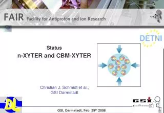
Test Results on the n-XYTER, a self triggered, sparcifying readout ASIC. Christian J. Schmidt et al., GSI Darmstadt. TWEPP 2007, Prague, Sept. 3. – 7. n-XYTER: DETNI Neutron Detector Readout ASIC. N eutron – X, Y, T ime and E nergy ... Readout. 8 LVDS output lines at 4 x 32MHz:

E N D
Test Results on the n-XYTER, a self triggered, sparcifying readout ASIC Christian J. Schmidt et al., GSI Darmstadt TWEPP 2007, Prague, Sept. 3. – 7.
n-XYTER: DETNI Neutron Detector Readout ASIC Neutron – X, Y, Time and Energy ... Readout 8 LVDS output lines at 4 x 32MHz: time stamp, channel no. + 1 differential, analogue output 128+1 asynchronous analogue inputs at 32 MHz total average input rate AMS CMOS 0.35µ with thick metal four 250 dies shared between DETNI and CBM collaboration n-XYTER was developed for neutron applications within EU FP-6 NMI3
n-XYTER: Novel FE-Chip Architecture Cast in Silicon Architectural Solution for FAIR CBM and PANDA. Starting point towards the development of the dedicated XYTER front-end ASIC for several FAIR applications. detector readout ASIC for high-density and high statistical rate time and amplitude measurement • 128 channels @ 50.7 µ pitch • freely running, self triggered autonomous hit detection • 850 (1000) ENC at 30 pF • dynamic range for 6 MIPs (300µ Si) • positive and negative signals • Per channel analogue energy and digital time stamp FIFO (1ns resolution) • De-randomizing, sparsifying Token Ring readout at 32 MHz
Channel layout overview, Clock Domains and Power time stampfast clock analogue domain no clock digital domain system clock total of 4 nF on chip MIM caps memory control ( 9 bit ) PDH reset comp analogue front end , PDH comp – TWCtrim reg analoguemem. maskreg. mono synch control tokencell ch.ID digitalmem. TSlatch clocktree PAD A/Dguard ring input MOSGND digitalBULK analogueGND& BULK analogueVDD comparatorVDD digitalGND digitalVDD 8 mm 5 mm
Data Driven Front-End: Asynchronous Channel Trigger detection of statistical, poisson distributed signals triggertimestamp reg. comparator Time WalkCompensationcircuit FASTshaper 18.5 ns peaking PDH reset chargepreamp dig. FIFO chargeinput SLOW shaper(2 stages) 140 ns peaking time Peakdetector & hold, free running pulse height output analogue FIFO Asynchronous registry and storage in 4-level fifo guarantees data loss < 4 % when read-out through token ring The DETNI ASIC 1.0, a front-end evaluation chip in AMS 0.35µ
Analogue Signal Sequence (Test Channel) Testpulse Release Slow Shaper Fast Shaper Discriminator Output
Tests on n-XYTER • 64/128 chan. connected • I²C-Interface • Test points accessible • All functional tests possible • Analogue evaluation possible One additional analogue test channel available for direct access of slow and fast shaper outputs...with output buffer would have been even more useful
Slow Control: 8Bit Registers accessible by I2C 16 mask registers with a mask bit for every channel 14 front-end adjustment registers for setting voltages and bias currents in the analogue part of the chip 2 configuration/status registers 2 diagnostic counters: token lost and fifo-overflow 2 test-delay registers (very useful for id. of pickup-paths etc.) 1 shift register 129 bytes deep for local channel threshold trimming (bit 0 to 4) and individual selectable analogue channel shutdown (bit 5) 3 delay registers for LSB time-stamp generation and tuning
FAST channel SLOW channel ENC 26.9 e/pF + 200 e 12.7 e/pF + 233 e peaking timea (1% to 99%) 18.5 ns 139 ns Analogue Pulses, Peaking Time, Front-End Noise Engineered for 30 pF, giving (850 ) 1000 e 600 e pre-amp and shaper power consumption: 12.8 mW per channel; OK for neutrons!
Analogue Setup Registers Tested example pre-amp feedback biasing Expected (simulation): range: 0.928 – 1.651 V Measurement: range: 0.880 – 1.655 V Access to DACs via several current mirrors only. They introduce INL and shifts
Slow Shaper Output, the Energy Channel Measurements on the test channel #129 varying input capacitance varying input charge
Testability and Diagnostics Individual analogue test channel Built in test pulse generator Programmable mask for every channel Programmable, forced trigger of PDH for every channel (check signal pedestal) Programmable dead time Diagnostic counters for pile-up and token statistics Backup Previsions / Safety Every individual channel may be shut off Clock signals derived on chip may be fed in separately Time stamp clock may be reduced without change of readout clock Override of on chip band-gap reference foreseen Various parts may be shut off In addition to global threshold, 5 bit programmable local threshold Experimental Built-in Safety-Belts with First Submission
Token Ring Readout Process token cycle token cell control logic for data readout or token pass Analog FIFO Disc. Timestamp FIFO data readout bus skip channels without data, asynchronously rush through empty channels until data found • Focus bandwidth where there is data • 32 MHz data readout • Automatic zero suppression (sparsification)
Token Ring Architectural Pros/Cons • High Efficiency • Empty channels automatically skipped in readout process • Built-in fair distribution of readout bandwidth, automatic bandwidth focussing • Built-in De-Randomization: 100% bandwidth used on data • Error Robustness • Any problematic channel (e.g. continuously firering) will divert and occupy a maximum of 1/nth of the bandwidth. • Built-in, non-perfect readout probability avoids unrecoverable logic deadlock: Problematic situations like any kind of pile-up, logic hang-ups or glitch cause mere deadtime but the “show will go on”. But: Data needs to be tagged with a time-stamp Data needs to be resorted and re-bunched after readout
Digital output of the n-XYTER No Valid Data Pattern DataValid Marker
Token Ring Readout, Data Transmission DataValid Four Data Elements Transmitted Ch 1, 8, 30, 82 TS grey coded Ch# grey coded data transfer tested at 35 MHz, will also work at 128 MHz
Analogue Differential Output, the Energy Channel Three signals, one signal altered Signal settling upon successive data
Power Consumption • preamplifier 7.4mW • fast shaper 2.5mW • slow shaper stage 1 1.7 mW • slow shaper stage 2 2.5 mW • discriminator 2.1 mW • peak detector and hold 2.7 mW • analogue FIFO 2.3 mW overall we find about 21 mW/channel
Some Inter-Channel Pick-Up, Ongoing Detective Work Cin = 0 pF, bond wire removed Cin = 22 pF • System Effect • No dependence upon no. of bond wires, power or gnd • May be worsened with discriminator settings (TWC) • So far the effect could not be simulated!
Some In-Channel Discriminator Feedback Detected ...upon removal of discriminator-power decouppling correlates with trigger These issues are particularly important with the self triggered architecture! They will be addressed even more in the next engineering run.
Investigating Individual Channels, Triggerefficiency Trigger efficiency in Treshold Scan: The S-Curves Derivative gives image of noise! - Input of test pulses at fixed rate, - scan threshold while measuring detection rate
Trigger efficiency tested for all channels Channel number note bonded and non-bonded channels origin of 2 ch periodicity attributed to four fold pulser circuitry
Summary of Testing Status, Further Steps • Chip is fully functional: front-end, time-stamping, data transfer, slow control, test features, analogue and digital FIFOs, analogue output • No severe flaws surfaced ! Further testing: • Connect to silicon strips, and see real signals • Test of performance at higher clock frequencies (go from 50 MHz to 256MHz) • System investigation: Homogeneity of the chip • Outlook: Preparation of engineering run started (H. K. Soltveit, Heidelberg). Submission envisioned early 2008. Cost for the bag of chips: ~100 kEuro • Additional minor modifications for this engineering run: • cut on power where easily possible • expand dynamic range from 20 fC (6 MIPs) to 40 or 50fC. • address system issues for homogeneity and temp. co. • reduce in-channel spurious feedback
Near to mid term future – go prototyping Generic n-XYTER architecture finds broad applications within FAIR: Silicon Strips, High Rate GEM TPC as well as large area gas detectors • CBM STS prototype integration with readout electronics,... module prototyping • Daq chain development • Employment in a PANDA GEM TPC prototype (need 1000 chips). • Prototype beam tests Dedicated FAIR XYTER development initiated: work out specifications for FAIR Applications • Front-end S/N and bandwidth power needs • Radiation hardness • Analogue pulse height resolution and dynamics • Integration of modern, low power ADC on chip pure digital interface Meanwhile: n – XYTER will serve as the prototype for a data driven, self triggered readout ASIC in FAIR detector prototyping