Download
1 / 21
210 likes | 398 Vues
n- XYTER Front-End Boards. Christian J. Schmidt, GSI Darmstadt. CBM STS Workshop, Karelia, June 1 – 4, 2009. Data Driven Front-End: Asynchronous Channel Trigger. detection of statistical, poisson distributed signals. trigger timestamp reg. comparator. Time Walk Compensation circuit.

E N D
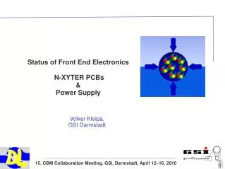
n-XYTERFront-End Boards Christian J. Schmidt, GSI Darmstadt CBM STS Workshop, Karelia, June 1 – 4, 2009
Data Driven Front-End: Asynchronous Channel Trigger detection of statistical, poisson distributed signals triggertimestamp reg. comparator Time WalkCompensationcircuit FASTshaper 18.5 ns peaking PDH reset chargepreamp dig. FIFO chargeinput SLOW shaper(2 stages) 140 ns peaking time Peakdetector & hold, free running pulse height output analogue FIFO Asynchronous registry and storage in 4-level fifo guarantees data loss < 4 % when read-out through token ring Read-out through balancing token ring 32 MHz data registry and read-out The DETNI ASIC 1.0, a front-end evaluation chip in AMS 0.35µ
"Simple" FEB for the n-XYTER Starter Kit • A simple hybrid PCB with signal fan-in, ADC and interconnect to SysCore DAQ chain • Allow development of the DAQ chain • Allow the readout of various detector prototypes, using the n-XYTER front-end chip
n-XYTER FEB: At the limits of PCB-technology Interference point of many technologies, each imposing limiting boundary conditions: • Chip-In-Board solution avoids space eating vias • allows pitch adaptation: • 50,7 µm on chip to • PCB side 101,4 µm on two levels • A simple hybrid PCB with signal fan-in, ADC and interconnect to SysCore DAQ chain
n-XYTER FEB Rev. C In spite of bonding difficulties, managed to realize • 10 Rev. C boards, fully functional • 4 rev. B boards with 64 channels functional (the other 64 may be employed for direct silicon det. tests) We are striving to get the entire system (FEB, SysCore, software) packaged to allow shipment. Starter kits in distribution Teams from Colcatta, Kiew, Dubna, Dubna (MPD), GSI, Heidelberg were introduced into running the starter kit with FEB and data chain at the GSI detector lab
Complex Mulitlayer Data Chain • Detector • n-XYTER-FEB • n-XYTER • FEB and Bonding Technology • Documentation (Manual, newest version this May with update on parameter description) • ADC • Interconnect • SysCore • Firmware • Embedded software • Soft configuration • Ethernet-Interconnect • PC and DAQ • KNUT • GUI • DAQ System DABC Software design freeze 1.7, firmware, software, knut Under heavy development (Anton Lymanets): low level diagnostic toolbox for system analysis to make successful deployment in other labs feasible
Additional: Mimicing Triggered Mode of Operation • Discussions with Petr Nomokonov revealed a nice and simple mode of forcing n-XYTER to operate classically in triggered mode: • Switch chip to test trigger mode • Switch off test pulse enable (important as would otherwise imply a special test mode) • Test trigger signal will sample all signals during monostable activity, window determined by "iota" parameter 120ns to several µs. • Alow to study noise all the way to the pedestal, where self triggered normal mode of operation would drown in triggers!
Test Trigger Mode alows globally triggered signal sampling test trigger input in test trigger mode triggertimestamp reg. comparator Time WalkCompensationcircuit FASTshaper 18.5 ns peaking PDH reset chargepreamp dig. FIFO chargeinput SLOW shaper(2 stages) 140 ns peaking time Peakdetector & hold, free running pulse height output analogue FIFO The DETNI ASIC 1.0, a front-end evaluation chip in AMS 0.35µ
n-XYTER FEBs • FEB-Rev D: next version to implement all learnings • Relieve PCB specs by tightening bonding necessities and challenge • Chip-In-Board, two layer bonding and metal in-lay cooling contact • GEM-TPC FEB: ongoing dual n-XYTER for PANDA GEM-TPC • n-XYTER Quattro: STS-Baby-Sensor double sided readout towards a beam telescope • Mid-term: Hybrid development for demonstrators (see Volker Kleipas talk tomorrow) • several n-XYTERs on Silicon-circuitboard
n-XYTER Quatro: Double Sided Silicon Readout • Read-Out of double sided Si, 256 x 256 channels • First setup to occupy complete capacities of one SysCore • Several Moduls may be set-up to make a beam telescope • FEE of both sides live on one potential! Rely upon readout-caps!
n-XYTER Quattro • four chips bonded on one board (Carmen Simons at GSI DetLab) • currently under tests • then: • bond a CBM baby sensor on one side only and test • bond both sides and test • We will make 4 = 3 +spare beam telescope elements for September beamtime at GSI
Feb Rev D, Layout – Start a new with Eagle Software Enhance availability of starter kits • Eagle allows script based layout • Generate real footprint • Much easier to follow nets • Easily make bond-plan • Input pitch 5.4 mils = 137µ • Max bonding angle 22° • Max bond length 3.4 mm • Targeted but may not be ready for beam-time
Preparation of Engineering Run (H.K. Soltveit) • Test Pulser • Identified very narrow line in test-pulse engine that introduces non-linearity of pulser • Cal setting changes power consumption 0 to 10mW implications to DC-level in current prototype through Temp Coeff. of shapers • Discriminator was designed as "above pedestal trigger" • not linear over full threshold span i.e. S-curves are non-linear, explains beamtime gain conundrum • Temperature coefficient in shapers addressed: • modification gives 0.2 mV/K, down from 20 mV/K, simulated 50 to 90°C • Observed Monostable crosstalk identified and addressed End of June 2009: Engineering run schematics review meeting End of July 2009: Submission readyness review meeting Then submission Expect chips in Sept/Oct.
Some In-Channel Discriminator Feedback Detected ...upon removal of discriminator-power decoupling correlates with internal discriminator trigger correlates with external test-pulse release signal (blue) These issues are particularly important with the self triggered architecture! They will be addressed even more in the next engineering run.
Investigating Individual Channels, Triggerefficiency Trigger efficiency in Treshold Scan: The S-Curves used to be the technique to get analogue signal information w/o ADC Caveat information on discriminator operation Derivative gives image of noise! This scale is not linear with pulse height, i.e. input charge! - Input of test pulses at fixed rate, - scan threshold while measuring detection rate
Thermographic Analysis: n-XYTER in Action • Chip temperature around 70°C on FEB with simple passive cooler • Digital readout and Time Stamp Clk Distribution surprisingly the hottest part
Conclusions • Starter Kits begin to become available • Feb Rev C+ fully bonded with SysCore • Feb Rev D high yield, fabricatable FEB • Data chain went through extensive debugging phase, currently software consolidating, tools for beam-time • Engineering run really in preparation, chips expected Sept./Oct. • many learnings addressed • future n-XYTER will be cured from child deseases and design-mishaps • black box operation much more feasible • n-XYTER on Silicon circuit board technology on the radar • parallel activity on CBM-XYTER development ongoing
New Detector Lab Facilities at GSI Construction of the new GSI Detector Lab has commenced! Located between GSI UNILAC and the CBM Offices (C27) • 600 m2 of climatized cleanroom space with relative humidity down to 20% • cleanroom class 10000 in general and better locally • dedicated bonding labs forseen • Additional 600 m2 available for detector testing, storage and other activities • Additional 100 m2 of high clearance (10m headroom), dedicated device setup space (detector integration and tests)