Download
1 / 44
500 likes | 899 Vues
Design of Low-Power Pipelined ADCs. By Ehsan Zhian-Tabasy Instructor Prof. S. M. Fakhraie This presentation is mostly based on two ISSCC06 conference papers:

E N D
Design of Low-Power Pipelined ADCs By Ehsan Zhian-Tabasy Instructor Prof. S. M. Fakhraie This presentation is mostly based on two ISSCC06 conference papers: [1] S.-T. Ryu, B.-S. Song, and K. Bacrania, “A 10b 50MS/s Pipelined ADC with Opamp Current Reuse,” ISSCC Dig. Tech. Papers, pp. 216-218, Feb. 2006. [2] T. Sepke, J. Fiorenza, C. G. Sodini, P. Holloway, and H.-S. Lee, “Comparator-Based Switched-Capacitor Circuits for Scaled CMOS Technologies,” ISSCC Dig. Tech. Papers, pp. 220-222, Feb. 2006.
Outline • Pipelined ADC Architecture • Novel Low-Power Pipelined ADCs • Opamp Current-Reuse Method [Ryu, ISSCC06] • Comparator-Based Switched Capacitor (CBSC) Method [Sepke, ISSCC06], [Fiorenza, JSSCC06] • Conclusion • References E. Zhian
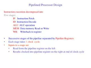
Pipeline ADC Architecture • What is an MDAC (Multiplying DAC)? E. Zhian
Opamp Current-Reuse SC MDAC Operation • Opamp is not used during the sampling phase. • Opamp Sharing: Use it for another stage • Switched Opamp: Power it down C C Reset input/output. C C bi*VREF VIN VRES VRES bi = {1, 0, -1} VOCM Sampling Phase (1) Amplification Phase (2) E. Zhian
Opamp Current-Reuse Opamp Sharing Technique [Nagaraj, JSSC97] • Save power and area, but summing node is never reset. C2 C1 VRES(n-1) VRES(n+1) C4 Sampling Amplification C3 bi+1*VREF Odd Phase Even Phase C2 C1 bi*VREF VRES(n) Amplification C4 Sampling C3 E. Zhian
Opamp Current-Reuse Switched-Opamp Technique [Waltari, JSSC01] • Power is turned off during the sampling phase. • Summing node is reset. • Useful for low voltage systems • Watch for turn-on delay and variable input capacitance. C 2C VIN 2 C 2 bi*VREF VRES 1 1 1 1: Sampling 2: Amplification E. Zhian
Opamp Current-Reuse Architecture Comparison 1 No power scaling is applied. 2 Except for [Yu, ISSCC96] 3 Watch for variable input capacitance. E. Zhian
on at 1 on at 2 • Opamp Current-Reuse Current Reusable Opamp [Ryu, ISSCC06] I I/2 I/2 VIP+ VIP– VO– VO+ VPB VPB Switched-opamp technique 1 2 VO– VO+ VNB VNB VIN+ VIN– VIN1+VIN1– VIN2+VIN2– I I Switching transient N- / P-input two opamps are stacked. Switch inputs rather than power down. E. Zhian
Opamp Current-Reuse MDAC during One Phase [Ryu, ISSCC06] VIPC bP*VREF P-input MDAC amplifies residue. CPS VIP+ CPF Vo– Vo+ CNF VIN+ N-input MDAC samples input & works as an active load. CNS bN*VREF VINC CMFB Odd Phase (1) E. Zhian
Opamp Current-Reuse MDAC during the Other Phase [Ryu, ISSCC06] VIPC bP*VREF P-input MDAC samples input & works as an active load. CPS VIP+ CPF Vo– Vo+ CNF VIN+ N-input MDAC amplifies residue. CNS bN*VREF VINC CMFB Even Phase (2) E. Zhian
Opamp Current-Reuse Opamp Current Reuse • Two opamps share bias current in different phases. • Reduce the number of opamps by half. • Power and area savings • Role switching rather than power down • No switching transient problem • Have two differential input pairs. • Summing node reset • Disadvantage • Additional current source stack • Reduce signal swing range. E. Zhian
Opamp Current-Reuse Interference from Sampling Side [Ryu, ISSCC06] Next stage VIPC CPS 1’ bP*VREF C CPF C Vo– Vo+ CNF VIN+ CNS q 1’ CMFB VINC VINC • Summing node changes while sampling. • Incomplete summing node settling • Injected charge on variable input capacitance E. Zhian
Opamp Topology • Opamp Current-Reuse Isolating Summing Nodes [Ryu, ISSCC06] VIPC VIPC bP*VREF CPS SP VIP+ CPF Vo– Vo+ VIN+ CNF SN CNS bN*VREF CMFB VINC VINC • Insert switch SN and SP. • Isolate the active load from the sampling node. • Gate node settles fast. E. Zhian
3-Bit MDAC • Opamp Current-Reuse Architecture for 10-Bit Pipelined ADC [Ryu, ISSCC06] 2 3 3 3b Flash 2b Flash 3b Flash 10 P-Input MDAC4 P-Input MDAC3 Digital Correction Logic N-Input MDAC1 N-Input MDAC2 In S/H 3 3b Flash 3b Flash 3 MDAC with opamp current reuse E. Zhian
Outline • Pipelined ADC Architecture • Novel Low-Power Pipelined ADCs • Opamp Current-Reuse Method • Comparator-Based Switched Capacitor (CBSC) Method • Conclusion • References E. Zhian
Note The output voltage needs to be accurate only at the sampling instant. No constraint how it gets to the final value! • Comparator-Based Switched-Cap. Motivation for CBSC Circuits • Traditional SC circuit design becomes extremely challenging in scaled technologies • Op-amp design issues • Low supply voltage Low output swing • Requires increased capacitance • Low device ro Low gain • Cascode gain stages • Exacerbates low swing problem • Cascade gain stages • Stability versus bandwidth/power tradeoff E. Zhian
Comparator-Based Switched-Cap. Proposed Solution • New class of comparator-based switched-capacitor circuit topologies • Eliminates op-amps • Utilizes architectures similar to op-amp based circuits • Amenable to scaled technologies E. Zhian
Comparator-Based Switched-Cap. Comparator-Based Switched-Capacitor Circuits (CBSC) • Example: switched-capacitor gain stage • Input sampling • Opamp-based charge transfer • Comparator-based charge transfer • Detailed charge transfer operation E. Zhian
Comparator-Based Switched-Cap. Sampling Phase (f1) • Open loop sampling • Input voltage sampled on C1 and C2 • f1A defines sampling instant • Minimizes signal dependent charge injection (Bottom-plate sampling) E. Zhian
Comparator-Based Switched-Cap. Opamp-Based Switched-Capacitor Gain-Stage • Charge Transfer Phase • Op-amp forces virtual ground condition • Exponential settling to virtual ground E. Zhian
Comparator-Based Switched-Cap. Comparator-Based Switched-Capacitor Gain-Stage • Charge Transfer Phase [Sepke, ISSCC06] • Comparator detects virtual ground condition • Comparator determines the sampling instant • Correct output voltage sampled on CL E. Zhian
Comparator-Based Switched-Cap. Charge Transfer Phase Details • Ensure Vx starts below VCM • Maximize accuracy of charge transfer • Maximize comparator decision time • Minimize final overshoot • Divide charge transfer (f2) into three sub-phases • Preset (P) • Coarse charge transfer (E1) • Fine charge transfer (E2) f1: Sample f2: Charge Transfer E. Zhian
Comparator-Based Switched-Cap. CBSC Charge Transfer Phase [Sepke, ISSCC06] • Preset (P) E. Zhian
Comparator-Based Switched-Cap. CBSC Charge Transfer Phase (cont’d) • Coarse charge transfer (E1) E. Zhian
Overshoot Correction • Comparator-Based Switched-Cap. CBSC Charge Transfer Phase (cont’d) • Fine charge transfer (E2) • Sampling switch (S) E. Zhian
Comparator-Based Switched-Cap. CBSC Applications • Applies to switched-capacitor circuits in general • Filters • Amplifiers • S-D converters • DACs • ADCs E. Zhian
Block Architectures • Comparator-Based Switched-Cap. Prototype 1.5b/stage Pipeline ADC [Sepke, ISSCC06] E. Zhian
Comparator-Based Switched-Cap. Comparator vs. Op-amp Summary • For the same power and speed • Noise bandwidth: 3 to 5x lower • Noise Power Spectral Density (PSD): 3.3x lower • Total: 10 to 15x lower mean-squared noise - or - • For the same SNR and speed • gm can be lowered 10-15x • gm versus ID relationship • Sub-threshold: • Strong inversion: • Potential for at least 10x power reduction E. Zhian
Comparator-Based Switched-Cap. CBSC: Pros and Cons • Pros • Potential for significant power reduction • Amenable to scaled technologies • Feedback and stability concerns removed • Applicable to wide range of SC circuits • Compatible with most known architectures • Cons • No output amplifier • Only switched-capacitor loads can be driven • Cannot simultaneously drive both sides of the sampling capacitor • Incompatible with closed-loop offset cancellation • Ramp linearity similar to finite gain in op-amp • Constant current source much easier to design • New technique • Not all issues are known yet E. Zhian
Die Photo ADCs Performance Summary (10-Bit 1.8V) E. Zhian
Conclusion Opamp Current-Reuse Method • Opamp current reuse technique • Two amplifiers in a single bias branch. • The number of opamps is reduced by half. • Achieve both power and area savings. • Switching two input paths • Summing node is reset. • There is no turn-on delay. • Further power reduction • Capacitive coupled gain-boosting amplifier • Use N-input amplifiers for N/P-cascode boosting. • Achieve speed while saving power. Comparator-Based SC Method • Presented new comparator-based switched-capacitor design methodology • Demonstrated 10b, 7.9MHz CBSC Pipeline ADC E. Zhian
References • [Fiorenza, JSSC06] J. Fiorenza, T. Sepke, P. Holloway, C. G. Sodini, and H.-S. Lee, “Comparator-Based Switched-Capacitor Circuits for Scaled CMOS Technologies,” IEEE J. Solid-State Circuits, vol. 41, no. 12, pp. 2658-5668, Dec. 2006. • [Nagaraj, JSSC97] K. Nagaraj, et al., “A 250-mW, 8-b, 52-Msamples/s Parallel-Pipelined A/D Converter with Reduced Number of Amplifiers,” IEEE J. Solid-State Circuits, vol. 32, pp. 312-320, March 1997. • [Ryu, ISSCC06] S.-T. Ryu, B.-S. Song, and K. Bacrania, “A 10b 50MS/s Pipelined ADC with Opamp Current Reuse,” ISSCC Dig. Tech. Papers, pp. 216-218, Feb. 2006. • [Sepke, ISSCC06] T. Sepke, J. Fiorenza, C. G. Sodini, P. Holloway, and H.-S. Lee, “Comparator-Based Switched-Capacitor Circuits for Scaled CMOS Technologies,” ISSCC Dig. Tech. Papers, pp. 220-222, Feb. 2006. • [Waltari, JSSC01] M. Waltari, and K. Halonen, “1-V 9-Bit Pipelined Switched-Opamp ADC,” IEEE J. Solid-State Circuits, vol. 36, no. 1, pp. 129-134, Jan. 2001. E. Zhian
Opamp Topology [Ryu, ISSCC06] VNG VPC VIP+ VIP- VPC VNG C1 P-Cascode Boost Amplifier C2 VO- VO+ N-Cascode Boost Amplifier C2 VNG VNC VIN+ VIN- C1 • Capacitive level shifting for N-input boosting amplifiers • Can achieve speed with low power. VNC VNG CMFB E. Zhian
Back Opamp Settling in Worst Condition [Ryu, ISSCC06] Standard Pipeline Output Node Sharing +Vref 0 –Vref • Design for opamp to settle with one more bit of resolution than required due to output node sharing. E. Zhian
Opamp Current-Reuse Tri-Level 3-Bit MDAC -1 -1 -1 0 -1 -1 0 0 -1 0 0 0 0 0 1 0 1 1 1 1 1 b2 b1 b0 Coarse 6 comparator levels -VREF 0 VREF 1 0 -1 1 0 -1 1 0 -1 C C C C • - + • + - Output Range C C C C 1 0 -1 1 0 -1 1 0 -1 -VREF 0 VREF Input Range E. Zhian
Back • Opamp Current-Reuse MDAC Operation in Both Phases [Ryu, ISSCC06] P-input MDAC amplifies residue. P-input MDAC samples input. VIPC VIPC VIP VREF’s VC VREF’s VIN VINC VINC VB CMFB Refresh N-input MDAC samples input. N-input MDAC amplifies residue. CMFB Sample Odd Phase Even Phase E. Zhian
Overshoot Correction [Sepke, ISSCC06] • Overshoot is predictable Vos1 E. Zhian
Back Overshoot Correction (cont’d) [Sepke, ISSCC06] • Overshoot is constant and predictable • Correction allows lower I2 and smaller Vos2 Vos1 Vos2 E. Zhian
Comparator Architecture [Sepke, ISSCC06] • Large gain obtained by cascading gain stages • Used in open-loop configuration only • No stability issues • First stage determines noise E. Zhian
Back Ramp Generation [Sepke, ISSCC06] • Current sources in prototype • Coarse charge transfer phase: I1 • Fine charge transfer phase: I2 I1 Current Source I2 Current Source E. Zhian
1.6 mm Sub-ADCs MDAC4 MDAC3 1.7 mm S/H MDAC1 MDAC2 Sub-ADCs CLK Die Photo (Opamp Current-Reuse Pipelined ADC) [Ryu, ISSCC06] E. Zhian
Back Prototype CBSC Pipeline ADC: Chip Micrograph [Sepke, ISSCC06] 0.18mm CMOS 0.4mm 2.9mm E. Zhian