Sequential Circuit Design: Principle
Sequential Circuit Design: Principle. Outline. Overview on sequential circuits Synchronous circuits Danger of synthesizing asynchronous circuit Inference of basic memory elements Simple design examples Timing analysis Alternative one-segment coding style

Sequential Circuit Design: Principle
E N D
Presentation Transcript
Sequential Circuit Design: Principle Chapter 8
Outline • Overview on sequential circuits • Synchronous circuits • Danger of synthesizing asynchronous circuit • Inference of basic memory elements • Simple design examples • Timing analysis • Alternative one-segment coding style • Use of variable for sequential circuit Chapter 8
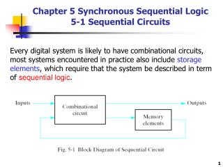
Overview on sequential circuit • Combinational vs sequential circuit • Sequential circuit: output is a function of current input and state (memory) • Basic memory elements • D latch • D FF (Flip-Flop) • RAM • Synchronous vs asynchronous circuit Chapter 8
D latch: level sensitive D FF: edge sensitive Chapter 8
Problem wit D latch:Can the two D latches swap data? Chapter 8
Timing of a D FF: Clock-to-q delay Constraint: setup time and hold time Chapter 8
Synch vs asynch circuits • Globally synchronous circuit: all memory elements (D FFs) controlled (synchronized) by a common global clock signal • Globally asynchronous but locally synchronous circuit (GALS). • Globally asynchronous circuit • Use D FF but not a global clock • Use no clock signal Chapter 8
2. Synchronous circuit • One of the most difficult design aspects of a sequential circuit: How to satisfy the timing constraints • The Big idea: Synchronous methodology • Group all D FFs together with a single clock: Synchronous methodology • Only need to deal with the timing constraint of one memory element Chapter 8
Basic block diagram State register (memory elements) Next-state logic (combinational circuit) Output logic (combinational circuit) Operation At the rising edge of the clock, state_next sampled and stored into the register (and becomes the new value of state_reg The next-state logic determines the new value (new state_next) and the output logic generates the output At the rising edge of the clock, the new value of state_next sampled and stored into the register Glitches has no effects as long as the state_next is stabled at the sampling edge Chapter 8
Sync circuit and EDA • Synthesis: reduce to combinational circuit synthesis • Timing analysis: involve only a single closed feedback loop (others reduce to combinational circuit analysis) • Simulation: support “cycle-based simulation” • Testing: can facilitate scan-chain Chapter 8
Types of sync circuits • Not formally defined, Just for coding • Three types: • “Regular” sequential circuit • “Random” sequential circuit (FSM) • “Combined” sequential circuit (FSM with a Data path, FSMD) Chapter 8
3. Danger of synthesizing asynchronous circuit • D Latch/DFF • Are combinational circuits with feedback loop • Design is different from normal combinational circuits (it is delay-sensitive) • Should not be synthesized from scratch • Should use pre-designed cells from device library Chapter 8
E.g., a D latchfrom scratch Chapter 8
4. Inference of basic memory elements • VHDL code should be clear so that the pre-designed cells can be inferred • VHDL code • D Latch • Positive edge-triggered D FF • Negative edge-triggered D FF • D FF with asynchronous reset Chapter 8
D Latch • No else branch • D latch will be inferred Chapter 8
Pos edge-triggered D FF • No else branch • Note the sensitivity list Chapter 8
Neg edge-triggered D FF Chapter 8
D FF with async reset • No else branch • Note the sensitivity list Chapter 8
Register • Multiple D FFs with same clock and reset Chapter 8
5. Simple design examples Follow the block diagram Register Next-state logic (combinational circuit) Output logic (combinational circuit) Chapter 8
D FF with sync enable Note that the en is controlled by clock Note the sensitivity list Chapter 8
T FF Chapter 8
Free-running shift register Chapter 8
Universal shift register 4 ops: parallel load, shift right, shift left, pause Chapter 8
Arbitrary sequence counter Chapter 8
Free-running binary counter Count in binary sequence With a max_pulse output: asserted when counter is in “11…11” state Chapter 8
Wrapped around automatically Poor practice: Chapter 8
Binary counter with bells & whistles Chapter 8
Decade (mod-10) counter Chapter 8
Programmable mod-m counter Chapter 8
6. Timing analysis • Combinational circuit: • characterized by propagation delay • Sequential circuit: • Has to satisfy setup/hold time constraint • Characterized by maximal clock rate (e.g., 200 MHz counter, 2.4 GHz Pentium II) • Setup time and clock-to-q delay of register and the propagation delay of next-state logic are embedded in clock rate Chapter 8