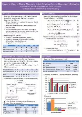
Experiments
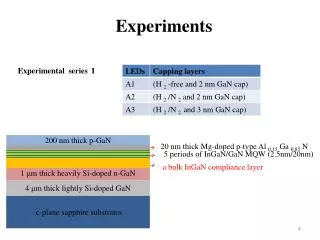
Experiments. Previous result (with ITO electrode). Experiments. Cr electrode ( Ohmic contact). Experiments. Cr electrode – after 300ºC,1hr annealing. Experiments. ZnO grown with Na citrate Carrier concentration: n-type, 3.1x10 18 /cm 3 ~ 9.9x10 18 /cm 3. Process conditions 1. Na ions

Experiments
E N D
Presentation Transcript
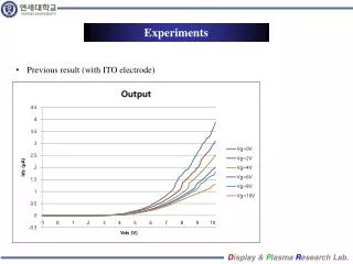
Experiments • Previous result (with ITO electrode)
Experiments • Cr electrode (Ohmic contact)
Experiments • Cr electrode – after 300ºC,1hr annealing
Experiments • ZnO grown with Na citrate • Carrier concentration: n-type, 3.1x10¹⁸/cm3~ 9.9x10¹⁸/cm3 • Process conditions • 1. Na ions • 2. High pH
Experiments • Na-doping on ZnO thin film → p-type conductivity
Future works New approaches for nanogap fabrication
Experiments Inclined UV photolithography 1 Photoresist Photoresist Removed (can be partially) 3 Au Nanowire growth Substrate Cr UV exposure Au Substrate Vacuum Deposition 2 Photoresist Cr Au Substrate
Experiments Inclined UV photolithography 1 Photoresist Au Substrate UV exposure Vacuum Deposition 2 Photoresist Cr Au Substrate
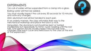
Experiments Photoresist curing : poor transmittance of slide glasses
Experiments Power problem: fixed PCB board – card contact problem
Nanogap fabrication by mechanical strain July , 30th 2010 Young Bum Yoo
CONTENTS Literature review Ideas Applications
Literature review Gap distance can be modulated by piezo element Used for characterize molecular junction (to overcome limit of e-beam lithography)
Literature review Strain induced by phase transformation Step structure to concentrate stress Hydrogenation temperature determines gap distance (a) 25ºC (b) 200ºC (c) 300ºC Volume expansion (α→β transformation) Induces ompressive strain Atomic diffusion from highly stressed region results nanogap formation
Literature review • Strained GaAsP by heteroepitaxy Strain released when AlGaAs is etched • Relaxation distance Notch breaking, nanogap formation
Literature review After undercut, nanogap formation Gap distance can be controlled by L (beam length)
Literature review Self organized nanowire By fracture approach Photoresist coating Vacuum deposition to form nanowire Crack by thermal cycling
Literature review Bulk material: Strain increases Tf Over critical Tf, total failure Thin film: Volume of strain energy released is smaller at bonded film Array of parrallel cracks can be easily produced by uniaxial strain
Literature review Cracks cannot penetrate already existing crack Easily fractureable photoresist (ex:AZ6612) 600nm thickness coating 90ºC annealing & dip into liquid nitrogen Thin films usually under tensile stress: After thermal cycle, gap is not closed
Literature review Crack spacing and angle are determined by stripe width Cracks cannot penetrate already existing crack Application as the hydrogen sensor is shown
Literature review Delamination: Substrate constraint leads stress concentration at the base of the crack Nanogap size is order of 100nm Delamination makes lift-off much easier Nanowire width can be further decreased by oblique angle deposition
Literature review Application as the nanowire transistor Application as the ZnO oxygen sensor Oscilliation: UV on-off for oxygen desorption Channel : TiOx nanowire (by anodizing Ti nanowire)
Literature review Literature review conclusion: Mechanical fracture can be used for nanogap fabrication Advantages – easy fabrication, controllable gap distance Problem is: Method is already researched and used well Hard to find originality Finding ideas with obtained inspiration: Materials & applications
Finding idea Residual tensile stress helps nanogap formation: Solution-processed thin film (Stressed by solvent evaporation) In case of sol-gel film: Cracking really happens in some cases There is a critical thickness that cracking initiates ex) ceria gel films 800nm 600nm
Finding idea Various type of crack can be formed by shrinkage-induced stress Pattern is dependent to film thickness and deposition parameters Ex) cracking of silica sol-gel thin film
Finding idea Sol-gel oxide films can be cracked and nanogap can be maintained 1. Thermal cycling Sol-gel film spin coating ↓ Annealing ↓ Dip into liquid nitrogen 2. Mechanical bending Sol-gel film spin coating (on kapton) ↓ Low-temp. annealing ↓ Mechanical bending
Applications Electron emission device Luminescent image SCE array
Finding idea Application into alignment layer: for multidomain uses Inserted polymer (PI,RM, or etc.) Regularly cracked silica Or solution-based re-filling: surface structure
Future work Hydrothermal growth from nanogap 1. Bridging from nanogap or 2. Inversed structure
Future work For device applications, Hydrothermal inactive, schottkey metal : nanowire growth direction Diode or piezoelectric device can be fabricated