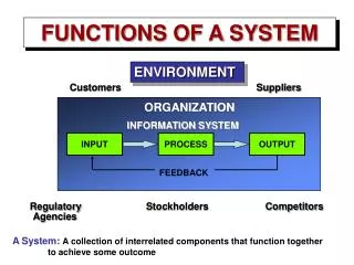
Understanding Input Stages in CMOS: Transition Times, Termination, and Practices
This document explores the critical aspects of input stages in CMOS technology, focusing on transition times, termination practices, and common pitfalls in data sheets. It covers rise and fall time limits, hysteresis effects, and waveform measurement techniques. Insights are provided on the importance of proper termination, the practice of using pull-up/down resistors, and the necessity of careful case studies to ensure device specifications are met. Recommended conservative margins and real-world examples underscore the complexity of interfacing CMOS with older logic families and the implications for design.


Understanding Input Stages in CMOS: Transition Times, Termination, and Practices
E N D
Presentation Transcript
Input Stages - Introduction • Most CMOS inputs have rise/fall time limits • Most inputs also have some hysteresis • Typical symbols in specifications tR, tTLH - rise time tF, tTHL - fall time tT - transition time • Waveform measurement • typically from 10% to 90% but not always • sometime parameter measurement method is not specified
Input Stages - Practice • Data sheets may list a parameter for information only and not 100% tested • Laboratory devices have shown that not all qualified devices will meet the data sheet • One case was when a part was shrunk • Migration to a faster process • Oscillations observed • Conservative margins recommended
Input Stages - Termination • Floating CMOS inputs are, in general, 'bad.' • Totem-pole currents, oscillations, etc. • Some devices offer pull-up/down resistors • SX-S only active during power transistions • Xilinx resistors controlled by SRAM • Care on internal tri-state lines • get example from XQR4000XL • Dedicated Inputs • Actel unused inputs were handled by s/w • Not true for some SX, SX-S clocks Check each case carefully
Input Transition TimesReferences • [1] ACT ™ 1 Field Programmable Gate Arrays, March 1991. • [2] ACT 1 and ACT 2 Military FPGAs, April, 1992. • [3] ACT ™ 1 Series FPGAs, April 1996. • [4] Radiation‑Hardened FPGAs, v3.0, January 2000. • [5] ACT ™ 2 Series FPGAs, April 1996. • [6] Accelerator Series FPGAs – ACT ™ 3 Family, September, 1997. • [7] 54SX Family FPGAs RadTolerant and HiRel, Preliminary V1.5, March 2000. • [8] HiRel SX-A Family FPGAs, Advanced v.1, April 2000. • [9] RT54SX-S RadTolerant FPGAs for Space Applications, Advanced 0.2, November, 2000. • [10] QPRO XQR4000XL Radiation Hardened FPGAs, DS071 (v1.1) June 25, 2000. • [11] QPRO™ Virtex™ 2.5V Radiation Hardened FPGAs, DS028 (v1.0) April 25, 2000 Advance Product Specification. • [12] Not in data sheet. • [13] Configurable Logic Data Book, Atmel, August 1995. • [14] AT6000LV, Atmel, October 1999.
Transition Time RequirementsImplications - Pullup Resistors • Often used for tri-state or bi-directional busses • Rise time (10% - 90%) = = 2.2 RC • Example C = 50 pF R = 10 k (keep power levels reasonable) = 500 ns violates many devices' specifications (see table)
Transition Time RequirementsImplications - Filters and Protection Circuits • Often used on signals • Elimination of noise • ESD protection • Etc. • RC filters or clamps (high C) can often substantially degrade transition times • Consider discrete hysteresis buffers, particularly for clock signals
One Bus Hold Circuit Bus Hold Circuit in an FPGA Supplies leakage current only.
Transition Time RequirementsImplications - Interfacing with older logic families • Case Study (1) • CD4000B CMOS NOR gate • VDD = 5V • tT (typ) = 100 ns • Case Study (2) • CD4050B (used as a level shifter, for example) • VDD = 5V • tT (max, 25 C) = 160 ns
Transition Time RequirementsImplications - Interfacing with older logic families (cont'd) • Case Study (3) - 54HC00 CMOS NOR gate • 5962-8403701VDA, NAND GATE, QUAD 2-INPUT Test Symbol Test conditions 1/ Limits Unit -55°C TC+125°C Min Max unless otherwise specified Transition time, tTHL, TC = +25C VCC=2.0 75 output rise and tTLH CL = 50 pF VCC=4.5 15 ns fall 3/ See figure 4 VCC=6.0 13 TC = -55C, -55C VCC=2.0 110 CL = 50 pF VCC=4.5 22 ns See figure 4 VCC=6.0 19 3/ Transition time (tTLH, tTHL), if not tested, shall be guaranteed to the specified limits in table 1.
Transition Time RequirementsParameter Measurement From: Figure 4, 5962-8403701VDA, NAND GATE, QUAD 2-INPUT
Transition Time RequirementsCase Study: RH1020 • Production Parts • Input stage was modified for clock upset • VCC = +5VDC • T=25°C • CLKBUF monitored on output • Because of design of the buffer, difficult to see effects on the input pin • Used a low-impedance signal generator, triangle waveform • Commercial specification is tR, tF of 500 ns • RH1020 did not meet this specification • SMD 5962-90965 does not specify this parameter
Transition Time RequirementsCase Study: RH1020 CLKBUF Notes • Conditions: Room temp; VCC = 5.0 V. • Oscillations detected consistently at tR = 360 ns • Sporadic output pulses at tR = 300 ns • Transition time requirement not symmetric • Oscillations detected consistently at tF = 1.5 s • Sporadic output pulses observed at tF = 1.0 s
Interfacing - Voltage Margin • TTL CMOS • Problem with discrete circuits (still seen) • Normally not a problem with 5V FPGAs • Issue with new FPGAs • 0.35 m may only pull up to 3.3 VDC • 0.25 m may only pull up to 2.5 VDC • Can be issue with parts having a VIH = 70% VDD • Ringing can cause false triggering • VIL = 0.8V and fast devices are sensitive to ringing on a backplane.
Inputs: RT54SX16 tT RT54SX16 output (bottom trace) with a slow rising input (top trace) which clocks a divide by two counter resulting in a "glitch." The clock input was provided by an HP8110A pulse generator.
Inputs: RT54SX16 tT RT54SX16 output (bottom trace) with a slow rising input (top trace) which clocks a divide by two counter resulting in a "glitch." The clock input was provided by an HP8110A pulse generator.
JTAG and Loss of Control • Run TCK with TMS=‘1’ • Guaranteed to return to TEST_LOGIC_RESET state within 5 clocks. • Share system clock with TCK • JTAG Hit • Inputs turn to outputs • Clock pin turns to output, clamps system clock No TCK, system hangs.