ATLAS Trigger/DAQ Read-Out-Buffer (RobIn) Prototype
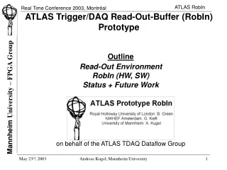
ATLAS Trigger/DAQ Read-Out-Buffer (RobIn) Prototype. Outline Read-Out Environment RobIn (HW, SW) Status + Future Work on behalf of the ATLAS TDAQ Dataflow Group. 40 MHz. 75 kHz. ROD. ~2 kHz. EFP. EFP. EFP. EFP. T/DAQ Architecture. Trigger. DAQ. Calo MuTrCh. Other detectors.

ATLAS Trigger/DAQ Read-Out-Buffer (RobIn) Prototype
E N D
Presentation Transcript
ATLAS Trigger/DAQ Read-Out-Buffer (RobIn) Prototype • Outline • Read-Out Environment • RobIn (HW, SW) • Status + Future Work • on behalf of the ATLAS TDAQ Dataflow Group
40 MHz 75 kHz ROD ~2 kHz EFP EFP EFP EFP T/DAQ Architecture Trigger DAQ Calo MuTrCh Other detectors 40 MHz D E T R/O LV L1 FE Pipelines 2.5 s ROS Lvl1 acc = 75 kHz RoI Read-Out Drivers RoI data = 2% 120 GB/s 120 GB/s RRC H L T D A T A F L O W ~ 10 ms ROD-ROB Connection R/O S Y S T E M LVL2 RoI Builder ROB RoI requests Read-Out Buffers L2 Supervisor L2 N/work L2 Proc Unit ROIB L2SV RR ROD-ROS Merger IOM L2N L2P I/O Manager ~3+3 GB/s Lvl2 acc = ~2 kHz Dataflow Manager E V B EBN Event Building N/work DFM ~ sec Event Filter SFI ~3 GB/s Sub-Farm Input Event Filter Processors EFN Event Filter N/work SFO EFacc = ~0.2 kHz Sub-Farm Output ~ 200 Hz ~ 300 MB/s
Prototype RobIn accepts 2 ROLs per Board Target Implementation accepts 4 ROLs GbE GbE … … … RoBin ROBin ROBin ROBin ROBin ROBin PCI PCI GbE GbE Concentrator switch GbE GbE GbE GbE ROS Baseline Total of ~1600 Read-Out-Links (RRC/ROLs) I/O Optimisation still to be done ROLs ROLs
ROS IOM (PC based) RobIn’s Request Handlers Control, error Requests (L2, EB, Delete) Trigger Request Queue = Process on PC = Linux Scheduler Fragments GbE = Thread PCI
Direct Connection (No IOM) Requests (L2, EB, Delete) RobIn’s . . . GbE Fragments
RobIn Requirements Summary • Functions: RECEIVE – BUFFER – DELIVER – RELEASE • Multiple S-LINK Input, max. 160MB/s per link, XOFF Capability • Embedded version due to mechanical constraints • Local buffer to compensate trigger latency • Efficient buffer management • PCI and GbE Interfaces for control and data requests • In-situ firmware upgrades, Test facilities, JTAG • Optional stand-alone mode (PCI disabled) • Standard Parameters: • 1kB fragment size (avg.), 75 kHz input event rate • ~ 3 kHz L2 request rate, ~ 3 kHz EB rate
PowerPC Module GbE Interface Virtex2 FPGA Mezzanine Connector Not shown: ROL Interface (TLK2501) SD-RAM Buffer PLX 64Bit PCI Interface Rapid Prototyping: MPRACE
RobIn Block Diagram, Component View • Hardware assistance for input provided by FPGA (DF-CORE) • Management task suitable for CPU (AUX-CORE) • Main data-path doesn't touch CPU
Common Part FIFO comms 100MHz 125MHz 66MHz “Slice“ Part (1..n) RobIn Block Diagram, Functional View • CPU controls common functions and serialises access to shared components (MAC, PCI) • FPGA provides parallel implementation of ROB-”Slices” Manages 64k pages Logical pages ~1kB
Network ROL2 ROL1 RobIn • 64Bit/66Mhz PCI, 3.3V supply (3V+5V signalling level) • 12 Layer PCB, Size 220*107mm, Test Connectors • Unit Cost: ~1400€ Buffers FPGA CTL PCI CPU
Board Control • Board supervised by CPLD XC95288XL • Programmable Reset Generation • Flash-Eeprom (for FPGA) programming via serial (JTAG-like) protocol • External access via connector • Access for one of PLX, PPC, FPGA • FPGA power-on configuration (slave SelectMap) • Path to external JTAG connector for factory programming and test • Few LEDs • Global System Clock: 66MHz for CPU, MAC, PCI, FPGA
ROL Embedded S-LINK • Unidirectional data transfer, with XOFF on return channel • Pluggable Optical Transceiver • TLK2501 2.5Gbit/s SerDes, 16 Bit + 2 Flags @ 125MHz • Link protocol engine in FPGA (CERN core) • 2.5GBit/s => 160MB/s forward, XOFF backward, links status • ROS Format • Start-of-Packet Control word • Header Data, with L1ID • End-of-Packet Control Word • Extra: Link can be re-configured as LSC => Loopback testing
Buffer • Cover Trigger Latency of ~ 10ms => 1.6MB required • 64MB SD-RAM => 400ms • Good SD-RAM performance requires bursts: • Block oriented Dual-Port Emulation provides sufficient BW
PCI • PLX PCI9656 PCI Bridge • 64 bit PCI, up to 66MHz • 32 bit local bus @ 66MHz, Multiplexed A/D • FIFO-buffered PCI-DMA, controlled from PLX or local master (FPGA) for Request Messages • Fifo-buffered “Direct Master Mode” (FPGA writes into host memory) for Response Messages • Fragment buffers are pre-allocated in host memory • Physical buffer address provided to RobIn with request • Data transferred via “Direct Master” into host memory, first data word (offset 0) set to “1” to indicate activity • End-of-transfer signalled via start-of-header marker (offset 0) written after data block completed
PCI Performance Current: With Master Mode DMA, Old: No Master Mode DMA Required for event data per ROL: ~ 10MB/s
Network I/F • Intel IXF1002 GbE MAC • Separate 32 bit RX, TX buses @ 66MHz • 16 bit control interface • VLAN support • 2kB TX-, 4kB RX-FIFO • Marvell Alaska 88E1011S GbE PHY • Dual Media Interface for Copper and Fibre • RJ45 Connector • Pluggable Optical transceiver
FPGA • Xilinx Virtex-2 XC2V1500-FF896 (XC2V2000 possible) • Recent 0.15µ FPGA technology, 1.5V core voltage • Logic: 15000 LUTs • 48 blocks of embedded memory (18kbit), 16 used for FIFOs • Hardware Multipliers (not used) • 8 Clock managers for DLL, Frequency Synthesis, 6 used • Up to 8 global on-chip clocks, 5 used • On-chip driver termination (DCI) for high-speed signals (ROL) • 528 I/O pins, all in use (including TEST connectors) • Easily reconfigurable for different scenarios
Processor • IBM PowerPC PPC405CR (375 MIPS @ 266MHz) • I+D Cache (16/8 kB) • SD-RAM @ 133MHz • External bus @ 66MHz, DMA • 64 MB SD-RAM Memory (same as for Buffer) • Boot ROM: 8MB Flash • Serial Interface (debug terminal) • I2C Interface (EEPROM for local configuration) • FPGA resources memory mapped to external bus • < 1W Power Consumption • Code compatible to PPC405GPr (400MHz), PPC405 in Virtex-2Pro (400MHZ)
Software • Tools • GCC, GDB + JTAG Debugger • OS possible (Linux, VxWOrks) • ROM resident Monitor + Loader (128kB): • Peek(), Poke(), Printf(), Getc(), Malloc(), Free(), LoadApp() • Application program • Page-level buffer manager for 64k Pages (75 kHz): • Used Page FIFO, Free Page Fifo + Free Page Stack • L1ID Hashing, Page Management List • Request Handling (~7kHz): Input Queues, Output DMA • Network Message Translation: Raw Socket Format • Operational monitoring • Local Configuration (e.g. number of ROLs, Media selection) • Application Coding in “C” => simplify code migration into FPGA • Small Code Footprint, < 16kB for core functions expected
Processor: Access to Resources Management Memory FPGA
Status • Hardware • 10 RobIn Boards available since March 03 • PCI Master Mode: √ • Buffer Memories: √ • Processor: √ • Network RX, TX/DMA: √ • ROL LDC Core: √ • ROL Handling and Page Manager: Simulation OK • Very close to put everything together
Status cont’ • Software • ROM Monitor + Terminal: √ • Application Code • Page Management: √ • Request Handling: 80% • PCI Request / Response Scheme: √ • Network Translation: 60% • Monitoring: 60% • ROS Software • Device Library + Driver √ • Fragment Processing API √ => ROS Baseline • Direct Connect: No special SW required
Future Work • June 03: RobIn Application and VHDL complete • Sept 03: Performance Testing and Optimisation, incl. Bus/Network I/O Optimisation • Dec 03: Design evolution: ROL media selection (fiber / copper) , number of ROLs, component modifications, Packaging • May 04: Final prototypes ready