Download

1 / 49
490 likes | 685 Vues
Analog to Digital Converters. Byron Johns Danny Carpenter Stephanie Pohl Harry “Bo” Marr October 4, 2005. Presentation Outline. Introduction: Analog vs. Digital? Examples of ADC Applications Types of A/D Converters A/D Subsystem used in the microcontroller chip

E N D
Analog to Digital Converters Byron Johns Danny Carpenter Stephanie Pohl Harry “Bo” Marr October 4, 2005
Presentation Outline • Introduction: Analog vs. Digital? • Examples of ADC Applications • Types of A/D Converters • A/D Subsystem used in the microcontroller chip • Examples of Analog to Digital Signal Conversion • Successive Approximation ADC
First Presenter Byron Johns
Analog Signals Analog signals – directly measurable quantities in terms of some other quantity Examples: • Thermometer – mercury height rises as temperature rises • Car Speedometer – Needle moves farther right as you accelerate • Stereo – Volume increases as you turn the knob.
Digital Signals Digital Signals – have only two states. For digital computers, we refer to binary states, 0 and 1. “1” can be on, “0” can be off. Examples: • Light switch can be either on or off • Door to a room is either open or closed
Examples of A/D Applications • Microphones - take your voice varying pressure waves in the air and convert them into varying electrical signals • Strain Gages - determines the amount of strain (change in dimensions) when a stress is applied • Thermocouple – temperature measuring device converts thermal energy to electric energy • Voltmeters • Digital Multimeters
Just what does an A/D converter DO? • Converts analog signals into binary words
Analog Digital Conversion 2-Step Process: • Quantizing - breaking down analog value is a set of finite states • Encoding - assigning a digital word or number to each state and matching it to the input signal
Step 1: Quantizing Example: You have 0-10V signals. Separate them into a set of discrete states with 1.25V increments. (How did we get 1.25V? See next slide…)
Quantizing The number of possible states that the converter can output is: N=2n where n is the number of bits in the AD converter Example: For a 3 bit A/D converter, N=23=8. Analog quantization size: Q=(Vmax-Vmin)/N = (10V – 0V)/8 = 1.25V
Encoding • Here we assign the digital value (binary number) to each state for the computer to read.
Accuracy of A/D Conversion There are two ways to best improve accuracy of A/D conversion: • increasing the resolution which improves the accuracy in measuring the amplitude of the analog signal. • increasing the sampling rate which increases the maximum frequency that can be measured.
Resolution • Resolution (number of discrete values the converter can produce) = Analog Quantization size (Q) (Q) = Vrange / 2^n, where Vrange is the range of analog voltages which can be represented • limited by signal-to-noise ratio (should be around 6dB) • In our previous example: Q = 1.25V, this is a high resolution. A lower resolution would be if we used a 2-bit converter, then the resolution would be 10/2^2 = 2.50V.
Sampling Rate Frequency at which ADC evaluates analog signal. As we see in the second picture, evaluating the signal more often more accurately depicts the ADC signal.
Aliasing • Occurs when the input signal is changing much faster than the sample rate. For example, a 2 kHz sine wave being sampled at 1.5 kHz would be reconstructed as a 500 Hz (the aliased signal) sine wave. Nyquist Rule: • Use a sampling frequency at least twice as high as the maximum frequency in the signal to avoid aliasing.
Overall Better Accuracy • Increasing both the sampling rate and the resolution you can obtain better accuracy in your AD signals.
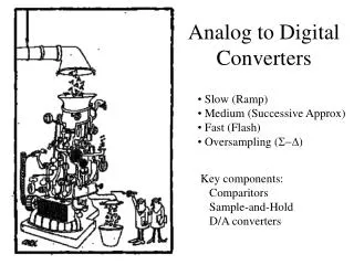
A/D Converter Types By Danny Carpenter • Converters • Flash ADC • Delta-Sigma ADC • Dual Slope (integrating) ADC • Successive Approximation ADC
Flash ADC • Consists of a series of comparators, each one comparing the input signal to a unique reference voltage. • The comparator outputs connect to the inputs of a priority encoder circuit, which produces a binary output
How Flash Works • As the analog input voltage exceeds the reference voltage at each comparator, the comparator outputs will sequentially saturate to a high state. • The priority encoder generates a binary number based on the highest-order active input, ignoring all other active inputs.
Advantages Simplest in terms of operational theory Most efficient in terms of speed, very fast limited only in terms of comparator and gate propagation delays Disadvantages Lower resolution Expensive For each additional output bit, the number of comparators is doubled i.e. for 8 bits, 256 comparators needed Flash
Sigma Delta ADC • Over sampled input signal goes to the integrator • Output of integration is compared to GND • Iterates to produce a serial bit stream • Output is serial bit stream with # of 1’s proportional to Vin
Advantages High resolution No precision external components needed Disadvantages Slow due to oversampling Sigma-Delta
Dual Slope Converter Vin • The sampled signal charges a capacitor for a fixed amount of time • By integrating over time, noise integrates out of the conversion • Then the ADC discharges the capacitor at a fixed rate with the counter counts the ADC’s output bits. A longer discharge time results in a higher count tFIX tmeas t
Advantages Input signal is averaged Greater noise immunity than other ADC types High accuracy Disadvantages Slow High precision external components required to achieve accuracy Dual Slope Converter
Successive Approximation ADC By Stephanie Pohl • A Successive Approximation Register (SAR) is added to the circuit • Instead of counting up in binary sequence, this register counts by trying all values of bits starting with the MSB and finishing at the LSB. • The register monitors the comparators output to see if the binary count is greater or less than the analog signal input and adjusts the bits accordingly
Advantages Capable of high speed and reliable Medium accuracy compared to other ADC types Good tradeoff between speed and cost Capable of outputting the binary number in serial (one bit at a time) format. Disadvantages Higher resolution successive approximation ADC’s will be slower Speed limited to ~5Msps Successive Approximation
Successive Approximation Example • 10 bit resolution or 0.0009765625V of Vref • Vin= .6 volts • Vref=1volts • Find the digital value of Vin
Successive Approximation • MSB (bit 9) • Divided Vref by 2 • Compare Vref /2 with Vin • If Vin is greater than Vref /2 , turn MSB on (1) • If Vin is less than Vref /2 , turn MSB off (0) • Vin =0.6V and V=0.5 • Since Vin>V, MSB = 1 (on)
Successive Approximation • Next Calculate MSB-1 (bit 8) • Compare Vin=0.6 V to V=Vref/2 + Vref/4= 0.5+0.25 =0.75V • Since 0.6<0.75, MSB is turned off • Calculate MSB-2 (bit 7) • Go back to the last voltage that caused it to be turned on (Bit 9) and add it to Vref/8, and compare with Vin • Compare Vin with (0.5+Vref/8)=0.625 • Since 0.6<0.625, MSB is turned off
Successive Approximation • Calculate the state of MSB-3 (bit 6) • Go to the last bit that caused it to be turned on (In this case MSB-1) and add it to Vref/16, and compare it to Vin • Compare Vin to V= 0.5 + Vref/16= 0.5625 • Since 0.6>0.5625, MSB-3=1 (turned on)
Successive Approximation • This process continues for all the remaining bits.
Pin: 7 6 5 4 3 2 1 0 Port E (analog input) ADR1 - result 1 Analog Multiplexer ADR2 - result 2 Result Register Interface A/D Converter ADR3 - result 3 ADR4 - result 4 ADC Flow Diagram in HC11 • 8 channel/bit input • VRL = 0 volts • VRH = 5 volts • Digital input on PE
Stuctural Diagram of ADC on HC11 PE0 AN0 PE1 AN1 PE2 AN2 PE3 AN3 PE4 AN4 PE5 AN5 PE6 AN6 PE7 AN7 ANALOG MUX 8-bits CAPACITIVE DAC WITH SAMPLE AND HOLD VRH SUCCESSIVE APPROXIMATION REGISTER AND CONTROL VRL INTERNAL DATA BUS MULT SCAN CCF CD CC CB CA ADCTL A/D CONTROL RESULT REGISTER INTERFACE ADR1 ADR2 ADR3 ADR4 P 64 M68HC11 Family Data Sheet
E Clock cycles: ADC by Clock cycle Conversion Sequence Sample (12) Bit 7 (4) 6 (2) _ (2) 0 (2) End (2) ADPU = 1 Successive approximation 1st, ADR1 2nd, ADR2 3rd, ADR3 4th, ADR4 CCF 0 32 64 96
HC11 => 8 bits => 28 = 256 • HC11 accepts 0 – 5V range • Voltage Range = (VRH– VRL)/255 * State
0 0 0 0 0 Bit: 7 6 5 4 3 2 1 0 ADCTL Register$1030 CCF |No Op| SCAN |MULT | CD | CC | CB | CA 0 Read 0 0 - • CCF: (1) after conversion cycle, (0) when written to. • SCAN: Continuous (1) or Not (0) • MULT: Multi-Channel (1) or Single Channel (0) • 0 = Single Channel is read 4 times • CD:CC:CB:CA = 0000 – 0111 Chooses input channel • Chooses Channel Group when MULT = 1 • Pg 27 – 28 in Reference Manual
1 0 0 1 0 0 Bit: 7 6 5 4 3 2 1 0 Options Register$1039 ADPU |CSEL | IRQE |DLY | CME | NoOp| CR1 | CR0 1 - • ADPU: Power up (1) wait 100ms, No conversion (0) • CSEL: use internal system clock (1), use E-clock (0) • IRQE: Falling Edge interupt (1), low level interrupt (0) • DLY: Delay enabled (1), Delay disabled (0) • CME: Monitor Clock (1), Don’t monitor clock (0) • CR[1:0] = Divide E clock by 1, 4, 16, 64. • pg 38 in reference manual
0 0 0 0 1 0 Bit: 7 6 5 4 3 2 1 0 Analog to Digital Results Register: $1031 - $1034 ADR2 ($1032) 0 0 • Register $1032 = $02 • Options Register ($1039) = $80 • ADCTL Register ($1030) = $00 • Just read in signal between 19.2 – 39.0 mV on pin E1!
CSEL OPTION ($1039) ADPU IREQ DLY CME 0 CR1 CR2 SCAN MULT CD CC CB CA ADCTL ($1030) CCF 0 OPTION EQU $1039ADCTL EQU $1030ADR1 EQU $1031ADRESULT RMB 1 Turn on charge pump and select clock source ORG $2000 LDAA #$80 ;ADPU=1,CSEL=0 STAA OPTION ; “ Delay for charge pump to stabilize LDY #30 ;delay for 105 ms DELAY DEY BNE DELAY Set ADCTL to start conversion • LDAA #$10 ;SCAN=0,MULT=1,CHAN GRP=00 • STAA ADCTL ; start conversion • LDX #ADCTL ;check for complete flag BRCLR 0,X #$80 * ;CCF is bit 7 Wait until conv. complete • LDAA ADR1 ;read chan. 0 STAA ADRESULT ;store in result SWI Read result
References • Ron Bishop, “Basic Microprocessors and the 6800”, Hayden Book Company Inc., 1979 • Motorola, “MC68HC11E Family Data Sheet”, Motorola, Inc., Rev. 5, 2003. • Motorola, “MC68HC11 Reference Manual”, Motorola, Inc., Rev. 4, 2002. • Motorola, “MC68HC11 Programming Reference Guide”, Motorola, Inc., Rev. 2, 2003.