Download
1 / 26
2.81k likes | 7.86k Vues
Computer System Architecture By M . Morris Mano Lecturer: Waqar A. Khan Email: waqarkhan4u7@hotmail.com Cell Num: 03345111163. Class Overview. First Course in Computer Hardware Learn how a computer actually works Build the “ Mano Machine”

E N D
Computer System Architecture By M. Morris Mano Lecturer: Waqar A. Khan Email: waqarkhan4u7@hotmail.com Cell Num: 03345111163
Class Overview • First Course in Computer Hardware • Learn how a computer actually works • Build the “Mano Machine” • Learn one computer in detail, others are mastered easily. • Homework: • Solve the even number of problems • Due at the beginning of the next class
8 Student Types • Insecure: 25 % • Silent: 20 % • Independent: 12 % • Friendly: 11 % • Obedient: 10 % • Heroic: 9 % • Critic: 9 % • Unmotivated: 4 % - Michigan State University
1-1 Digital Computers • Computer Architecture • Refers to those attributes of a system visible to a programmer or those attributes that have a direct impact on the logical execution of a program • Computer Organization • Refers to the operational units and their interconnections that realize the architectural specifications • Examples • Architectural attributes includes the instruction set, I/O mechanism and addressing memory • Organizational attributes includes hardware details transparent to the programmer • Hint: {Arch: whether computer perform multiply, organization: simple multiply or addition}
Application S/W API Operating System ROM BIOS Computer H/W 1-1 Digital Computers • Program(S/W) • A sequence of instruction • S/W = Program + Data • The data that are manipulated by the program constitute the data base • Application S/W • DB, word processor, Spread Sheet • System S/W • Consist, collection of software whose purpose is more effective usage of computers. • OS, Firmware, Compiler, Device Driver • How application software is differ from system software?
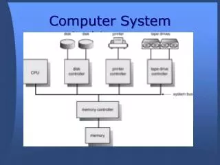
1-1 Digital Computers • Computer Hardware • CPU • Memory • Program Memory(ROM) • Data Memory(RAM) • I/O Device • Interface: 8251 SIO, 8255 PIO, 6845 CRTC, 8272 FDC, 8237 DMAC, 8279 KDI • Input Device: Keyboard, Mouse, Scanner • Output Device: Printer, Plotter, Display • Storage Device(I/O): FDD, HDD, Memory CPU Input Device Interface Output Device Figure 1-1 Block Diagram of a digital Computer
1-1 Digital Computers • 3 different point of view(Computer Hardware) • Computer Organization(Chap 1 - 4) • H/W components operation/connection • Computer Design(Chap 5 - 7) • H/W Design/Implementation • Computer Architecture(Chap 8, 9, 11, 12) • Structure and behavior of the computer as seen by the user • Information format, Instruction set, memory addressing, CPU, I/O, Memory
1-1 Digital Computers • What is “Computer Architecture”? - Hennessy and Patterson, Computer Organization and Design(1990) • Computer Architecture • Instruction Set Architecture (ISA) • Machine Organization • “ISA”? • Instructions, Addressing modes, Instruction and data formats, Register • “Machine Organization”? • CPU(Control, Data path), Memory, Input, Output
1-2 Logic Gates 0 : 0.5 1 : 3 • ADC(Analog to Digital Conversion) • Signal Physical Quantity Binary Information V, A, F, Discrete Value • Gate • The manipulation of binary information is done by logic circuit called “gate”. • Fig. 1-2 Digital Logic Gates • AND, OR, INVERTER, BUFFER, NAND, NOR, XOR, XNOR • George Boole • Born: 2 Nov 1815 in Lincoln, Lincolnshire, England • Died: 8 Dec 1864 in Ballintemple, County Cork, Ireland
x y z F 0 0 0 0 0 0 1 1 0 1 0 0 0 1 1 0 1 0 0 1 1 0 1 1 1 1 0 1 1 1 1 1 1-3 Boolean Algebra • Boolean Algebra • Deals with binary variable(A, B, x, y: T/F or 1/0) + logic operation(AND, OR, NOT…) • Boolean Function: variable + operation • F(x, y, z) = x + y’z • Truth Table: Fig. 1-3(a)Relationship between a function and variable • Logic Diagram: Fig. 1-3(b)Algebraic Expression Logic Diagram(gates로 표현) x y F 2n Combination Variable n = 3 z
Purpose of Boolean Algebra • To facilitate the analysis and design of digital circuit • Convenient Tools • Truth table : relationship between binary variables • Logic diagram : input-output relationship • Find simpler circuits for the same function • Boolean Algebra Rule : Tab. 1-1 - Operation with 0 and 1: x + 0 = x , x + 1 = 1 , x • 1 = x , x • 0 = 0 - Idempotent Law: x + x =x , x • x = x - Complementary Law: x + x' = 1 , x • x' = 0 - Commutative Law: x + y = y + x , x • y = y • x - Associative Law: x + (y + z) = (x + y) + z , x • ( y • z) = (x • y) • z - Distributive Law: x • ( y+ x) = (x • y) + (x • z) , x + (y • z) = (x + y) • (x + z) - DeMorgan's Law: (x + y)' = x' • y’ , (x • y )’ = x’ + y’ General Form:(x1 + x2 + x3 + … xn)' = x1' • x2' • x3' • … xn’ (x1 • x2 • x3 • … xn) ' = x1' + x2' + x3' + … xn’
[Examples] • F= ABC + ABC’ + A’C = AB(C + C’) + A’C = AB + A’C 1 inverter, 1 AND gate 감소 Fig. 1-6(a) • [Examples] • F= AB’ + C’D + AB’ + C’D = x + x (let x= AB’ + C’D) = x = AB’ + C’D Fig. 1-6(b) • Fig. 1-4 2 graphic symbols for NOR gate (a) OR-invert (b) invert-AND x y z x y z (x+y+z)’ x’y’z’ • Fig. 1-5 2 graphic symbols for NAND gate (a) AND-invert (b) invert-OR x y z x y z (xyz)’ (x’+y’+z’)
1-4 Map Simplification • Karnaugh Map(K-Map) • Map method for simplifying Boolean expressions • Minterm / Maxterm • Minterm : n variables product ( x=1, x’=0) • Maxterm : n variables sum (x=0, x’=1) • 2 variables example • F =x’y + xy m0 + m1 + m2 + m3 M0 M1 M2M3 m1 m3 (m1 + m3) (Complement = M0 M2)
C B A B A C D • 3 variables • 4 variables • Map • 2 variables B A • 5 variables C B A D E F
y x (1) Truth Table (2) • [Example] F= x + y’z (3) z F= x + y’z
Adjacent Square • Number of square = 2n (2, 4, 8, ….) • The squares at the extreme ends of the same horizontal row are to be considered adjacent • The same applies to the top and bottom squares of a column • The four corner squares of a map must be considered to be adjacent • Groups of combined adjacent squares may share one or more squares with one or more group
C C B B A A B B A A C C D D • [Example] • F=AC’ + BC • [Example] • F=C’ + AB’ • [Example] • F=C’ + AB’ • Product-of-Sums Simplification F=B’D’ + B’C’ + A’C’D F’=AB + CD + BD’(square marked 0’s) F’’(F)=(A’ + B’)(C’ + D’)(B’ + D) Sum of product Product of Sum
NAND Implementation • Sum of Product : F=B’D’ + B’C’ + A’C’D • NOR Implementation • Product of Sum : F=(A’ + B’)(C’ + D’)(B’ + D) • Don’t care conditions • F(A,B,C)=(0, 2, 6), d(A,B,C)= (1, 3, 5) • F=A’ + BC’= (0, 1, 2, 3, 6) B’ D’ C’ A’ D A’ B’ C’ D’ D’ B X X X A C
1-5 Combinational Circuits • Combinational Circuits • A connected arrangement of logic gates with a set of inputs and outputs • Fig. 1-15 Block diagram of a combinational circuit • Analysis • Logic circuits diagram Boolean function or Truth table • Design(Analysis) • 1. The Problem is stated • 2. I/O variables are assigned • 3. Truth table(I/O relation) • 4. Simplified Boolean Function(Map andBoolean Algebra Use) • 5. Logic circuit diagram i f 0 0 i f Combinational Circuits (Logic Gates) 1 1 . . . . . . i f n m Experience
y y x x z z • Design Example : Full Adder • Full adder is a combinational circuits that forms the arithmetic sum of three input bit(Carry considered) • 3 Input(x, y, z), 2 Output(S: sum, C: carry) • Truth Table • 4. Simplification • S=xy’z’ + x’y’z + xyz + x’yz’ • = z’(xy’ + x’y) + z(x’y’ + xy) • = z’(x y) + z(x y)’ • =a’b + ab’ (let a=z, b=x y) • =x y z • C= xy’z + x’yz + xy • =z(xy’ + x’y) + xy • =z(x y) + xy • 5. Logic circuit diagram x y z c s (x y)’=(xy’+x’y)’ =(x’+y)(x+y’) =x’x+x’y’+xy+yy’ =x’y’+xy
1-6 Flip-Flops Combinational Circuit = Gate Sequential Circuit = Gate + F/F • Flip-Flop • The storage elements employed in clocked sequential circuit • A binary cell capable of storing one bit of information • SR(Set/Reset) F/F • D(Data) F/F • “no change” condition: Q(t+1)=D • Solutions: 1) Disable Clock 2) Feedback output into input • JK(Jack/King) F/F • JK F/F is a refinement of the SR F/F • The indeterminate condition of the SR type is defined in complement • T(Toggle) F/F • T=1(J=K=1), T=0(J=K=0) if the JK F/F • Representation Formula: Q(t+1)= Q(t) T
Positive clock transition ts th • Edge-Triggered F/F • State Change : Clock Pulse • Rising Edge(positive-edge transition) • Falling Edge(negative-edge transition) • Setup time(20ns) • minimum time that D input must remain at constant value before the transition. • Hold time(5ns) • minimum time that D input must not change after the positive transition. • Propagation delay(max 50ns) • time between the clock input and the response in Q
Race Phenomenon • Condition - Setup time > Propagation delay • Symptoms- 0 and 1, then repeatUnstable one state is • Solution- Edge triggered F/F orMaster/Slave F/F use • Examples • 7470 : J-K Edge triggered F/F • 7471 : J-K Master/Slave F/F • Excitation Table • Required input combinations for a given change of state • Present State with Next State 1 : Set to 1 0 : Complement 1 : Clear to 0 0 : No change Don’t Care
Input Combinational Circuit Output Flip-Flops Clock 1-7 Sequential Circuits Combinational Circuit = Gate Sequential Circuit = Gate + F/F • A sequential circuit is an interconnection of F/F and Gate • Clocked synchronous sequential circuit • Flip-Flop Input Equation • Boolean expression for F/F input • Input Equation Examples • DA = Ax + Bx, DB = A’x • Output Equation • y = Ax’ + Bx’ • Fig. 1-25 Example of a sequential circuit DA x A A’ DB B B’ Clock y
State Diagram • Graphical representation of state table • Circle(state), Line(transition), I/O(input/output) Input Equ. = Next State • State Table • Present state, input, next state, output Expression • Design Example: Binary Counter Next State = Output • x=1: 00, 01, 10, 11, 00, 01, ….. x=0: no change • State Diagram: 4 state(00, 01, 10, 11) • Excitation Table(2 bit counter = 2 F/F)
B B B B A A A A x x x x • Logic Diagram • Map for simplification • Input variable: A, B, x KA JA 1 X X X X X XXX 1 KA=Bx JA=Bx KB JB 1 1 1 1 X X X X X X X X KA=x JB=x • 1. The Problem is stated • 2. I/O variables are assigned • 3. Truth table(I/O relation) • 4. Simplified Boolean Function • 5.Logic circuit diagram • Sequential Circuit Design Procedure • 1-5 (see Section) (Combinational Circuit Design) • Sequential Circuitin the process 3 State diagramorState tableutilization • F/F Number: 2m+n(m – State Number, n - Input Number)
![Computer Architecture & Operating System [O.S.]](https://cdn0.slideserve.com/35278/computer-architecture-operating-system-o-s-dt.jpg)