Noise Mitigation Strategies in LV Circuits: Solutions for Improved Grounding
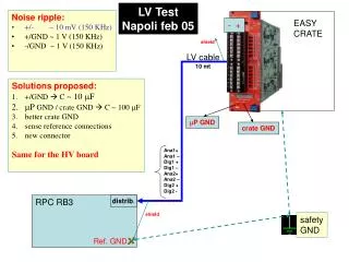
This document presents findings and proposed solutions for addressing noise and ripple in low voltage (LV) circuits. Testing conducted in Napoli on February 5 revealed significant noise levels, with observed ripples +/- 10 mV (150 KHz) and ground fluctuation of +/- 1 V. Proposed methods include enhanced grounding techniques, improved capacitance at various points, and the introduction of new connectors for consistent references across the system. The focus is on optimizing the grounding design for the LV distribution boards and ensuring shielded connections for safety.


Noise Mitigation Strategies in LV Circuits: Solutions for Improved Grounding
E N D
Presentation Transcript
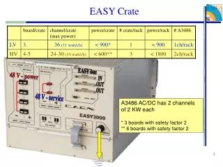
EASY CRATE - + mP GND Ana1+ Ana1 – Dig1 + Dig1 – Ana2+ Ana2 – Dig2 + Dig2 - crate GND LV Test Napoli feb 05 • Noise ripple: • +/- ~ 10 mV (150 KHz) • +/GND ~ 1 V (150 KHz) • -/GND ~ 1 V (150 KHz) shield LV cable 10 mt • Solutions proposed: • +/GND C ~ 10 mF • mP GND / crate GND C ~ 100 mF • better crate GND • sense reference connections • new connector • Same for the HV board RPC RB3 distrib. shield safety GND Ref. GND
Rack LV 4 pairs LV distrib. board chip chip From LV power supply with floating output ALV1 AGND1 DLV1 ALV DGND1 shielded cable AGND ALV2 AGND2 DLV DLV2 DGND2 DGND shield IRON – MAGNET safety ground AGND FEB 1 chip chip AGND FEB strip copper chip kapton AGND Double Gap 2 Double Gap 1 DGND Chamber metallic structure AGND FEB 6 HVReturn Copper 2 Copper 1 chamber GND