Simplified Transistor - Transistor Logic (TTL)
Simplified Transistor - Transistor Logic (TTL). Transistor - Transistor Logic (TTL) Simplified form of inverter Two instead of four transistors Two instead of four resistors For low v i input, output v o is high Q 1 is on ( saturation ).

Simplified Transistor - Transistor Logic (TTL)
E N D
Presentation Transcript
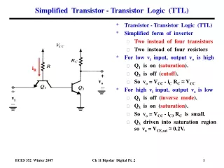
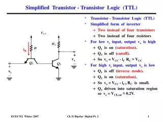
Simplified Transistor - Transistor Logic (TTL) • Transistor - Transistor Logic (TTL) • Simplified form of inverter • Two instead of four transistors • Two instead of four resistors • For low vi input, output vo is high • Q1 is on (saturation). • Q3 is off (cutoff). • So vo = VCC - iC RC≈VCC • For high vi input, output vo is low • Q1 is off (inverse mode). • Q3 is on (saturation). • So vo = VCC - iC3 RCis small. • Q3driven into saturation region so vo = VCE,sat≈0.2V. iR + vo vi Ch 11 Bipolar Digital Pt. 2
Simplified Transistor - Transistor Logic (TTL) • Assumptions for analysis: • All transistors are npn and identical. • For p-n junctions in transistors to be conductingcurrent, • VBE or VBC must be 0.7V or higher. • For smaller junction voltages, current flow is negligibly small. • For transistors in forward active mode, • iC = βiB, • VBE,active≈ 0.7 V • For transistors in forward saturation mode, • VBE,sat≈ 0.8 V. • VCE,sat≈ 0.2 V. • iC < βiB or iC / iB < β. • For transistors in inverse mode (E junction reverse biased, C junction forward biased), • current gain is very small • iE = βriB • βr is very small, e.g. βr ~ 0.02 vo vi Ch 11 Bipolar Digital Pt. 2
Simplified Transistor - Transistor Logic (TTL) Low Input, High Output Load inverter • For low vi input, output vo is high • Q3 of driving inverter is in saturation so vo = VCE,sat = 0.2 V = vi of Q1 • Transistor Q1 (Load Inverter) • E jcn forward biased (VBE1 = 0.7 V ). • C jcn only weakly forward biased (VBC1 = ? ). • Q1 in saturation (VCE1= VCB1 + VBE1 = -VBC1 + VBE1≈ -0.45V + 0.7V = 0.25V) and iC1 < βiB1. • Transistor Q3 (Load Inverter) • How do we find VBC1? • VB1 = VBC1 + VBE3 = 0.9 V • Assuming VBC1≈ VBE3 , then both = 0.45 V • So E jcn of Q3 forward biased,but not enough so iB3≈ 0 and Q3 is off (iC3≈ 0). • RC iC3≈ 0 and vo≈ VCC = 5 V. • Current iR flows through R and out the input • Size of iR? iR = (VCC - VB1 )/R = (5 V - 0.9 V)/4K=1 mA • Where does it go? • Virtually all of the current flows out emitter of Q1 , iR≈ iE1 = 1mA • This current flows into the collector of Q3. of the drive inverter (out the input). VCC = 5V VCC = 5V VB1 = 0.7V+0.2V = 0.9V iR Driving inverter R=4K . VBE1= 0.7V + p + + n VBC1 vo p + + n n iC1 VBE3 iE1 n vo=VCE,sat = 0.2 V I Q3 in saturation V 0.7 V Ch 11 Bipolar Digital Pt. 2
Simplified Transistor - Transistor Logic (TTL) High Input, Low Output • Q3 in driving inverter is in cutoff so vo = VCC = 5 V = vi of Q1 • Transistor Q1 (Load Inverter) • E jcn rev. biased (VBE1= 0.7V, VBE1< 0). • C jcn forward biased (VBC1 = ? ). • Q1 in inverse active mode and iE1 = βriB1 ≈ 0, since βr is very small, e.g. βr ~ 0.02 • Transistor Q3 (Load Inverter) • How do we find VBC1? • Know VB1 = VBC1 + VBE3 • Assuming iR flows through C junction of Q1 and into the base of Q3, then VBC1≈ VBE3≈ 0.7 V so iR = (VCC - VBC1 -VBE3)/R = (5 V- 1.4 V)/4K = 0.9 mA • So E jcn of load’s Q3 is forward biased, iB3≈ iR = 0.9 mA = 900 µA! • If Q3 in active mode, iC3 = βiB3 and for β = 50, then iC3 = 50(0.9 mA) = 45 mA. • Is this possible? NO! Why? vo= VCC - iC3 RC = 5 V - 45 mA (1.6K) = 5V - 72V = - 67V < 0 ! Not possible ! • So Q3 must be in saturation mode since the base current is very large (900 µA), where vo= VCE,sat ≈ 0.2 V; so iC3 =(5V-0.2V)/1.6K= 3mA. This verifies that Q3 is in saturation since iC3 = 3 mA < βiB3 = 45 mA. VCC = 5V VCC = 5V iR RC = 1.6K VB1 = 5 V-iRR Driving inverter Ic3 = 3 mA R=4K . + + p + VBC1 n VBE1< 0 vo n p Q3 in cutoff + n + iE1 ≈ 0 iC1 ≈ iB3 VBE3 n vo=VCC = 5 V I iC active Saturation iC/iB < V 0.7 V vCE Ch 11 Bipolar Digital Pt. 2
Simplified TTL Transfer Characteristic • Region I (A to B) (Low vi, high vo ) • Q1 is in forward saturation • E jcn forward biased (VBE1 = 0.7 V and base current is large, iB1 = iR1 = 1 mA ). • C jcn is weakly forward biased (VBC1 = 0.45 V ), so Q1 in saturation mode. • VCE1= VCB1+VBE1 = -VBC1+VBE1≈ -0.45 + 0.7 ≈ 0.25V • Current iR is flowing out the input. • Q3 is biased in forward active mode, but only weakly(not on since VBE3 < 0.7 V). • VB1 = vi + 0.7 V • Assuming VBC1≈ VBE3 , then both are equal to (0.35 V + vi /2) ~ 0.45V < 0.7 V. • So E jcn of Q3 is forward biased, but not enough so iB3≈ 0 and Q3 is off. • Then iC3≈ 0 and vo≈ VCC = 5 V. • Note • iR= (VCC – VCE3,sat –VBE1)/R = (5 V - 0.2V - 0.7V)/4K = 1.0 mA • Since iC1 = iB3≈ 0, nearly all of this current is going out the E of Q1 so iE1 ≈ iR = 1.0 mA. VCC = 5V VCC = 5V iR VB1 = 0.7V+vi RC = 1.6K R=4K . iC3 VBE1= 0.7V + + p + n VBC1 vo n p + n + iE1 iC1 = iB3 VBE3 n vi vo A B VCC = 5V I vi Ch 11 Bipolar Digital Pt. 2
Simplified TTL Transfer Characteristic • Region II (B to C) (Transition region) • Q1 is still in saturation. • Q3 initially is biased in forward active mode, but weakly(VBE3 < 0.7 V). • When does this change? • When vi = 0.6 V, then VB1 = vi + 0.7 V = 1.3 V so VBC1≈ VBE3 = 0.65 V and these p-n junctions canbeginto conductcurrent. • This current comes thru R as iR. • This provides the base current for Q3 to begin to turn on and so the collector current iC3 rises and the output voltage starts dropping according to vo= VCC - iC3 RC = 5 V - iC3 (1.6K) • Note the size of iR is about the same as before, i.e. iR = (VCC - VBC1 -VBE3)/R = (5 V- 1.3 V)/4K = 0.93 mA. Most of this current is still going out the gate input (E of Q1 ) since iB3 starts out very small (~μA’s). VCC = 5V VCC = 5V iR RC = 1.6K VB1 = 0.7V+vi R=4K . iC3 VBE1= 0.7V + p + n + VBC1 vo n p + n + iE1 -iC1 = iB3 VBE3 n vi vo A B VCC = 5V I II VCE3,sat = 0.2V C vi 0.6 V 0.7V Ch 11 Bipolar Digital Pt. 2
Simplified TTL Transfer Characteristic • Where is point C? • Region II (B to C) (Transition region) • Q1 initially in saturation • Q3 initially is biased in forward active mode, but only weaklyon since VBE3 < 0.7 V. • For Q3, as vi rises, the base current iB3 rises, iC3 rises and the output voltage drops. vo= VCC - iC3 RC = 5 V - iC3 (1.6K) • Where is point C? • When vi = 0.7 V, then VB1 = VBC1 + VBE3 = vi + 0.7 V = 1.4 V so VBC1≈ VBE3 = 0.7 V and these p-n jncs can conduct large currents. • As vi rises from 0.6 V to 0.7 V, more and more of iR (0.9 mA) goes into the base of Q3 and it enters further into the active mode. • At C, Q3 reaches the edge of saturation, vo = VCE,sat = 0.2 V, so iC3 = (5V - 0.2)/1.6K = 3 mA. Then iB3 = iC3 /β = 3mA/50 = 60 μA. So only 60 μA of iR (~ 1 mA = 1000 μA) needs to be diverted into the base of Q3 to drive it into saturation! • So at point C most of iR is still going out the gate’s input (E of Q1), since iR = 0.9 mA and iB3 = 60 μA. VCC = 5V VCC = 5V iR RC = 1.6K VB1 = 0.7V+vi R=4K . iC3 VBE1= 0.7V + + p + n VBC1 vo n p + n + -iC1 = iB3 VBE3 iE1 n vi vo iC Q3 A B VCC = 5V C active Saturation iC/iB < β I II VCE3,sat = 0.2V C A,B vi 0.6 V 0.7V vCE Ch 11 Bipolar Digital Pt. 2
Simplified TTL Transfer Characteristic • Region III (C to D) (Low output region) • Q1 initially still in saturation at C • As vi rises above 0.7V, VB1 is nearly constant at 1.4V, so E junction of Q1 becomes less forward biased and then eventually becomes reverse biased. • C junction is forward biased, so Q1moves from forward active to inverse active mode where iE1 = βr iB1 where βr = 0.02 << β = 50. • Q3 is entering saturation at C, VBE3≈ 0.7 V • For Q3, as vi rises above 0.7 V, VB1 rises slowly to 1.6 V as vi rises to 5 V. • When VB1≈ 1.6 V, then VBC1≈ VBE3 = 0.8 V = VBE.sat. • At VBE3 = 0.8 V, iB3 is larger yet and now Q3 is strongly driven into saturation so VCE3,sat 0.1 V. • For Q3 in saturation, iC3 << β iB3 . As iB3 increases, iC3 is nearly constant since vo = VCE3,sat and VCE3,sat goes down from 0.2 V to 0.1 V so iC3 increases from 3.0 mA to iC3 = (5V - 0.1)/1.6K = 3.06 mA. VCC = 5V VCC = 5V iR RC = 1.6K VB1 ≈ 1.4V R=4K iC3 . + + p + n VBE1 VBC1 vo n p + n + iC1 = iB3 VBE3 iE1 n vi vo iC Q3 A B C D VCC = 5V I II III active Saturation iC/iB < β 0.2V 0.1V C D A,B vi 0.6 V 0.7V 5 V vCE Ch 11 Bipolar Digital Pt. 2
Simplified TTL Transfer Characteristic VCC = 5V VCC = 5V • Noise Margin (Low state) • VOL = VCE3,sat = 0.1 V • VIL = 0.6 V • NML = VIL - VOL = 0.6V - 0.1 V = 0.5 V • Noise Margin (High state) • VOH = VCC = 5 V • VIH = 0.7 V • NMH = VOH - VIH = 5 V - 0.7 V = 4.3 V RC = 1.6K R=4K + + + VBE1 VBC1 vo + + VBE3 vi vo A B iC Q3 VCC = 5V C D . I II III NML = VIL - VOL active Saturation iC/iB < β NMH = VOH - VIH C D 0.2V VOL = 0.1V vi A,B 0.6V 0.7V 5 V VOL VIL VIH VOH vCE Ch 11 Bipolar Digital Pt. 2
Simplified TTL Propagation Delay • Output going high • Transistor Q3 turned off (cutoff) • Charging current flows through RC • tPLH is time it takes the output to rise from VOL = VCE,sat = 0.1 V to 1/2(VOH + VOL) = 2.6 V VCC = 5 V vo iRc iCap RC = 1.6K VCC + vo + C VCE + VBE VCE,sat t tPLH vo A B VOH = 5V I II III C VOL =0.1V D vi 0.6 V 0.7V 5 V VIL VIH Ch 11 Bipolar Digital Pt. 2
Simplified TTL Propagation Delay • Output going low • Transistor Q3 turned on (initially active, moving toward saturation) and providing discharge current (P R S) • But current also flows through RC • tPHL is time it takes the output to fall from VOH = VCC = 5 V to 1/2(VOH + VOL) = 2.6 V VCC = 5 V vo iRc iCap RC = 1.6K VCC + vo + C 2.6 V VCE + VBE VCE,sat t tPHL iC vo A B VOH = 5V I II III S R C VOL =0.1V D vi 0.6 V 0.7V 5 V VIL VIH P vCE Ch 11 Bipolar Digital Pt. 2
Simplified TTL Propagation Delay • Output going low vo VCC = 5 V iRc iCap RC = 1.6K VCC iC + vo + C 2.6 V + VCE VBE VCE,sat t tPHL iC S R P What current to use for the transistor Q3? vCE Ch 11 Bipolar Digital Pt. 2
Simplified TTL Propagation Delay • Output going low • Q3 starts in active mode at Pt. R • Final note: • iC = 45 mA is a very large current, which is useful for discharging the capacitor quickly. • When the capacitor is discharged, this iC3 drops dramatically in size to only • At this point, Q3 is now in saturation mode since vo VCC = 5V iRc iR RC = 1.6K iCap VCC + iB3 iC3 vo C + + VCE VBE VCE,sat t iC S R P vCE Ch 11 Bipolar Digital Pt. 2
Simplified TTL Power Dissipation • Output High State • Transistor Q3 is in cutoff so iC3 = 0, so no static power dissipationin Q3. • Transistor Q1 is in saturation with iB1 = iR = 1 mA • Static power dissipation for high state, PL1 =VCC iR = (5 V)(1 mA) = 5 mW • So static power dissipation for the inverter for the high output state is PH = 5 mW • Output Low State • Transistor Q3 is in saturation so v o = VCE,sat = 0.1 V. • iC3 = (VCC - VCE3,sat )/RC = (5V - 0.1 V)/1.6K = 3 mA. • PL3 =VCC iC3 = (5 V)(3 mA) = 15 mW • Transistor Q1 is in the inverse active mode, but still has a large base current of 0.9 mA. • PL1 =VCC iR = (5 V)(0.9 mA) = 4.5 mW • Total power dissipation in low state PL =19.5 mW • Average P = 1/2(PH + PL) = 12.3 mW • Power - Delay Product • DP = P tp =(12.3 mW)(8.3 nsec) = 102 pJ VCC = 5 V iCap RC = 1.6K iR iC3 + vo + C + VCE VBE vo A B VOH = 5V I II III C VOL =0.1V D vi 0.6 V 0.7V 5 V VIL VIH Ch 11 Bipolar Digital Pt. 2
Simplified Transistor - Transistor Logic * Simplified TTL provides performance similar to RTL. • Logic levels and noise margins • Noise Margin for Low State • NML = VIL – VO = 0.6 V - 0.1 V = 0.5 V • Noise Margin for High State • NMH = VOH - VIH = 5 V - 0.7 V = 4.3 V • Unequal noise margins for high and low states. • Propagation delays • Output going low • Output going high • Propagation delay • Power – Delay Product * Simplified TTL very similar to RTL in noise margins. * Better speed due to smaller RC used in simplified TTL (1.6 K) versus 10 K in RTL. * Simplified TTL worse in power dissipation and power-delay product. * Also more costly and complex due to use of more transistors per gate. Ch 11 Bipolar Digital Pt. 2
Simplified TTL vs. RTL * Logic levels and noise margins • Noise Margin for Low State • NML = VIL – VO = 0.6 V - 0.1 V = 0.5V • Noise Margin for High State • NMH = VOH - VIH = 5 V - 0.7 V = 4.3 V • Unequal noise margins for high and low states. • Propagation delays • Output going low • Output going high • Propagation delay • Power – Delay Product vo vo vi vi * Logic levels and noise margins • Noise Margin for Low State • NML = VIL – VO = 0.7 V - 0.2 V = 0.5 V • Noise Margin for High State • NMH = VOH - VIH = 5 V - 0.8 V = 4.2 V • Unequal noise margins for high and low states. • Propagation delays • Output going low • Output going high • Propagation delay • Power – Delay Product Ch 11 Bipolar Digital Pt. 2