Expanded Modes, Bus, External Memory
This document outlines the interfacing of external memory to the 68HC11 microcontroller, focusing on expanded modes of operation and bus timing. It includes a comparison between single-chip and expanded modes, detailing pin configurations and memory mapping. The text references Sections 4.1-4.7.3 of Huang's textbook, elaborates on in-class activities, and provides insights into timing conventions with practical examples. The content is essential for understanding the function and integration of external components in microcontroller applications. ###

Expanded Modes, Bus, External Memory
E N D
Presentation Transcript
Expanded Modes, Bus, External Memory • Today: • First Hour: Expanded Modes, Bus, Timing • Section 4.1-4.7.2 of Huang’s Textbook • In-class Activity #1 • Second Hour: Interfacing external memory to 6811 • Section 4.7.3 of Huang’s Textbook • In-class Activity #2
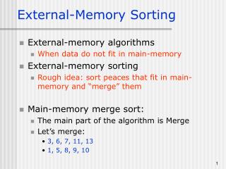
6811Operation Modes • Single chip mode: a mode in which the 68HC11 functions without external address and data buses. • The 68HC11 has 5 I/O ports (A, B, C, D, and E) to use in this mode. • Expanded mode: a mode in which the 68HC11 has the capability to access a 64KB address space. • Port B is used as the upper address signals (A15-A8) • Port C is used as time-multiplexed address/data bus (A7/D7-A0/D0). • Only three I/O ports are available for direct use. • Choosing modes: • MODB, MODA pins (look up PRG!) • (1,0) => single chip; (1,1) => Expanded
Expanded Mode PA7 PAI ROM-8KB PULSE ACCUMULATOR OC2 O PA6 C OC3 PA5 1 PORT PA4 OC4 RAM-256 bytes OC5 A PA3 IC1 PA2 PERIODIC INTERRUPT PA1 IC2 EEPROM-512 bytes COP WATCHDOG IC3 PA0 PE7 PD5 SS SCK PD4 PE6 SPI PE5 MOSI PD3 PORT PE4 PD2 MISO PORT DATA DIRECTION A/D E PE3 D CONVERTER PE2 PD1 TxD SCI PE1 RxD PD0 PE0 V REFH M68HC11 CPU V REFL ADDRESS DATA BUS RESET INTERRUPTS XIRQ IRQ HANDSHAKE I/O (V ) PPBULK DATA DIRECTION C XTAL PARALLEL I/O OSCILLATOR PORT B PORT C EXTAL E P P P P P P P P P P P P P P P P S S SINGLE MODA B B B B B B B B C C C C C C C C T T MODE CHIP LIR 7 6 5 4 3 2 1 0 7 6 5 4 3 2 1 0 R R SELECT MODB B A (V ) STBY A A A A A A A A A A A A A A A A AS 1 1 1 1 1 9 8 D D D D D D D D R/W 1 V EXPAND DD 5 3 2 1 0 7 6 5 4 3 2 1 0 4 POWER V SS
Expanded Mode 1 MODB 1 MODA E R/W AS 68HC11 A15-A8 PB7-PB0 Bus AD7-AD0 PC7-PC0 Other pins not shown
t t rise fall 1 90% V DD 0 10% V DD Timing Conventions Recap A real signal has nonzero rise and fall times 1 0 Single-signal waveform 1 0 Multiple-signal waveform
Timing Conventions Recap Unknown signals (when they are changing) representation unknown (a) Single signal unknown (b) multiple signals Unknown signals
Timing Conventions Recap A floating signal is represented by a level half way between logic high and low. Signal floating (a) Single signal Signals floating (b) multiple signals Floating signals
Crystal & E-clock Crystal clock: 8 MHz => One cycle = 125 ns XTAL 125 ns E clock: 2 MHz => One cycle = 500 ns E 500 ns
Bus Timing Diagram XTAL E R/W A15-A8 HI ADDR A7/D7-A0/D0 LO-ADDR DATA AS • Observe that AD lines active as address only for 1/2 E cycle • Most external memory devices need address lines active for 1E cycle • AS line to the rescue, combined with external address latch!
74373 Octal Transparent Latch with 3-State Outputs Positive edge triggered 11 CLK 11 LE 373 Stores an 8 bit number 18 19 H QH 17 16 G QG 14 15 F QF 13 12 /OE is active LO output enable Determines when register contents are visible at the outputs E QE 8 9 D QD 7 6 C QC 4 5 B QB 3 2 A QA OE 1 LE: Latch Enable. High => latch is transparent to data inputs
Latching the Address 1 MODB 1 MODA E R/W AS 68HC11 Address A0-A7 latched on the falling edge of AS A15-A8 PB7-PB0 Bus AD7-AD0 PC7-PC0 Other pins not shown D0-D7 LE 0 OE 373 Q0-Q7 A0-A7
Latching allows A7-A0 to be available for the second half of the E-clock cycle at the output of the latch Latching (contd) A0-A7 latched at falling AS edge 250 ns E AS 125 ns A7/D7-A0/D0 LO-ADDR DATA
Memory Mapping • Memory mapping external memory => can access external memory using normal instructions and memory addresses. • Similar to I/O memory mapping • Address space assignment • - Use only unallocated memory space • - Allocated in units of 2n KB (n is an integer) • Allocated space for the 68HC11A8 • $0000-$00FF: SRAM • $1000-$103F: I/O registers • $B600-B7FF: EEPROM • $E000-$FFFF: ROM
Consider an external 13-bit memory chip => 8KB Divide 64 KB space into eight 8KB blocks. Block number Address range $0000-$1FFF $2000-$3FFF $4000-$5FFF $6000-$7FFF $8000-$9FFF $A000-$BFFF $C000-$DFFF $E000-$FFFF 0 1 2 3 4 5 6 7 Memory Mapping Example Map external memory to: $4000-$5FFF
First four bits of memory map: 0100 or 0101 Partial decoding: A[15-13] = 010 Address Decoding Why is E connected to E3 ? 74LS138 O0 E1 O1 010 E2 External Memory O2 E E3 O3 O4 A15 A2 O5 A14 A1 O6 O7 A13 A0 Address decoder design
74LS138: E3: active high enable => Decoding done when E clock is high I.e at second-half of E-clock cycle Goal: Enable (chip select) external memory with the output (O2) of decode at this time I.e. at second-half of E-clock cycle Decoding (contd) Decoded values available E
8KB SRAM HM6264A • Two chip enable signals: • CS1 is active low • CS2 is active high. • WE: write enable • (active low) • OE: output enable • (active low)
Putting it together 74F138 PB7/A15 A2 PB6/A14 A1 O2 PB5/A13 A0 E E3 V E2 E1 DD 68HC11 CS2 CS1 74LS00 WE R/W 74LS04 PB4/A12 - A12-A0 PB0/A8 74F373 AS LE HM6264A O7-O0 AD7-AD0 D7-D0 OE OE I/O8 - I/O1
Revisit: Bus Timing Diagram XTAL E R/W A15-A8 HI ADDR A7/D7-A0/D0 LO-ADDR DATA AS Second half of E-cycle
During second-half of E-cycle CS1 asserted (from O2) E =1 during this time => R/W’ passed to WE’ Recall: (X.1)’ = X’ {NAND gate} In this case, X = (R/W’)’ {NOT gate} Latch output holds A0-A7 AD0-AD7 connected to I/O lines of SRAM Data sent back to port C if it is a READ Data sent from port C if it is a WRITE Putting it together (contd) Second half of E-cycle E
Do Activity #2 Now • Due: End of Class Today. • RETAIN THE LAST PAGE(S) (#3 onwards)!! • For Next Class: • Read Chapter 4 of Huang • Review all material, identify your problem areas, and Bring your questions! • Next week’s studio: Catch up with experiments. Summarize reading of Chapter 4, Chapter 5 (sections 5.1-5.4), and Chapter 6 (6.1 – 6.7)