Interfacing 3.3V CMOS SRAM: High Level Design and Functional Overview
This document provides a comprehensive overview of interfacing 3.3V CMOS SRAM, focusing on the construction and operational principles of a 128 x 8-bit memory chip. Key features include a clock cycle range of 10-20 ns, multiplexed address and data bus to minimize pin usage, and lower power consumption through chip deselect capabilities. Packaging options include 32-pin Plastic SOJ and Type II TSOP. A detailed truth table, timing diagrams, and a list of major SRAM manufacturers are included for reference.

Interfacing 3.3V CMOS SRAM: High Level Design and Functional Overview
E N D
Presentation Transcript
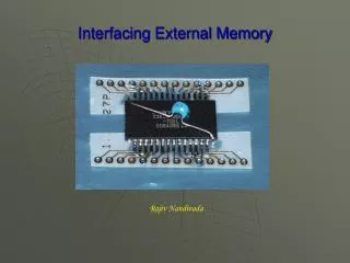
Interfacing External Memory Rajiv Nandivada
High Level Schematic • Clock cycle of 10-20 ns (Depending on its use). • 3.3 V CMOS SRAM (128 x 8 bit). • Uses multiplexed address and data bus to reduce the number of port pins. The lower address bits are held in latch while the data is transferred.
Functional Block Diagram of SRAM • Single 3.3 V supply. • Lower power consumption via chip deselect. • Available in 32 pin Plastic SOJ, and 32 pin Type II TSOP packages.
Pin Configuration SOJ and TSOP Top View SOJ: Small Outline J Leads TSOP: Thin Small Outline Package
Timing Diagrams Read cycle: Write cycle:
Major Manufacturers of SRAM • Alliance, • Brilliance • Crosslink • Cypress Semiconductor • Dense-PAC Micro • Etron Technology • Eureka • Hitachi • IBM • IDT • Mitsubishi • NEC • Samsung • Seiko Epson • Sharp • Sony • Toshiba
Electrically Erasable Programmable Read-only Memory (EEPROM)
I2C(Inter IC) Bus SDA: Serial Data Line SCL: Serial Clock Line
Packaging • SOJ or Small Outline J-lead • TSOP or Thin Standard Outline Package • DIP or Dual Inline Package • ZIP or Zigzag Inline Package • PLCC or Plastic Leaded Chip Carrier
Packaging Contd.. • SOJ or Small Outline J-lead • TSOP or Thin Standard Outline Package • DIP or Dual Inline Package • ZIP or Zigzag Inline Package • PLCC or Plastic Leaded Chip Carrier
Pricing Depends on • The type of package it comes in (DIP, SOJ, TSOP) • The speed of the memory. • The market value. • The vendor (Digikey, Jameco) • Storage capacity( 128K X 8, 256K X 8) • The type of memory (Flash, EEPROM)
References • www.cygnal.com • www.digikey.com • www.srams.co.uk • www.jameco.com • www.atmel.com • www.xicor.com