Download
1 / 1
10 likes | 161 Vues
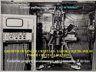
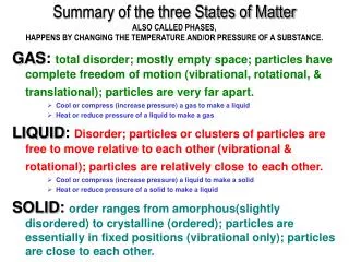
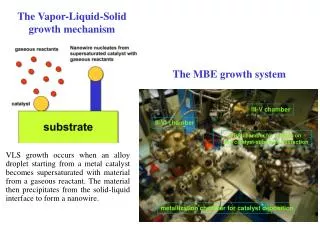
Figure 4b. Figure 4a. Figure 4c. Figure 4d. Vapor-Liquid-Solid Growth of ZnSiN 2. Alexander Grutter, Timothy Peshek, and Kathleen Kash Department of Physics, Case Western Reserve University. Crystal Growth, cont’d… Baked for twelve hours at 650 °C

E N D
Figure 4b Figure 4a Figure 4c Figure 4d Vapor-Liquid-Solid Growth of ZnSiN2 Alexander Grutter, Timothy Peshek, and Kathleen Kash Department of Physics, Case Western Reserve University • Crystal Growth, cont’d… • Baked for twelve hours at 650 °C • Cooled to room temperature under flowing ammonia • We analyzed the samples using optical microscopy, SEM, and energy-dispersive X-ray spectroscopy (EDS). The results of this investigation are shown in Figure 4. This preliminary evidence is highly suggestive of VLS ZnSiN2 growth. Abstract New types of semiconductors made of group II-IV-V2 elements, such as ZnSiN2 and ZnGeN2, are interesting for their optical, electric, and magnetic properties. To date, little work has been done to investigate these materials, especially in the case of ZnSiN2. ZnSiN2 is a wide band-gap (4.4 eV)1 semiconductor which forms a part of the ZnSiN2-ZnGeN2-ZnSnN2 alloy system, the II-IV-V2 analog to the very important AlN-GaN-InN system. ZnSiN2 growth has only been reported a few times to date, either by combining Zn3N2 and Si3N4 at high pressure (6 GPa)2 or by metal-organic vapor phase epitaxy (MOVPE)1, 3. We have designed and implemented a new vapor-liquid-solid (VLS) based technique for the synthesis of ZnSiN2. The system implements an atmospheric pressure growth process by dissolving vapor phase zinc and nitrogen into liquid phase silicon, allowing solid crystals to nucleate in this mix (vapor-liquid-solid!). At high temperatures, the high vapor pressure of Zn means that the placement of Zn pellets into the crystal growth chamber will provide the required Zn vapor. To introduce nitrogen, we rely on the decomposition of ammonia (NH3) that occurs on the surface of the liquid. System Design A diagram of the crystal growth system can be seen below in Figure 1: Figure 2 – The Si-Au phase diagram has an unusually large temperature drop at the eutectic, with the melting temperature dropping by over 700 ºC. Note the horizontal lines indicating the temperatures at which we tested the alloying of Au and Si and the temperatures at which we grew ZnSiN2. Figure 4 – Optical (4a), Energy Dispersive Spectroscopy (EDS) (4b), and SEM (4c, 4d) images reveal a new type of microstructure. Many hexagonal structures were found, indicating the growth of crystallites with hexagonal symmetry, most likely capped with hemispherical gold droplets. As the crystal structure of ZnSiN2 is a distorted wurtzite1, this is strong evidence of the formation of ZnSiN2.EDS reveals the presence of Zn, Si and N in these crystallites in concentrations consistent with stoichiometric ZnSiN2. Figure 1 – The ZnSiN2 growth system was designed to allow easy alteration of growth conditions. The system can be isolated by a series of valves, allowing us to change gas cylinders, pump down the system, or flow gases through the reactor at temperatures ranging from 20-1000 °C. Figure 3a Figure 3b Figure 3a – Optical microscope image of Si wafer after plating with Au Figure 3b – Optical microscope image of Au plated Si wafer after baking at 550 °C for 1.25 hours. Note the two distinct types of regions visible in the image. Figure 3c – Scanning electron microscope (SEM) image of the sample after baking. Note the phase separation of Au and Si as well as the uniformity of the matrix. • Conclusions • Crystallite structures exhibiting the hexagonal symmetry of ZnSiN2 have been grown by a VLS technique. • Chemical analysis is consistent with stoichiometric ZnSiN2 . • This will be the first reported growth of ZnSiN2 by this technique. • To demonstrate conclusively the presence of ZnSiN2, electron diffraction should be performed to measure the lattice constants. • References • A. Osinsky, V. Fuflyigin, L.D. Zhu, A.B. Goulakov, J.S. Graff, and E.F. Schubert, “New concepts and preliminary results for SiC bipolar transistors: ZnSiN2 and ZnGeN2 heterojunction emitters”, Proc. IEEE/Cornell Conf. High Performance Devices, pp. 168-172, August 7-9, Ithaca, NY (2000). • T. Endo, Y. Sato, H. Takizawa, and M. Shimada, “High-pressure synthesis of new compounds, ZnSiN2 and ZnGeN2 with distorted wurtzite structure”,J. Mat. Sci. Lett.11, 424 (1992). • 3. T. Cloitre, A. Sere, and R.L. Aulombard, “Epitaxial growth of ZnSiN2 single-crystalline films on sapphire substrates”, Superlatt. Microstruc. 36, 377 (2004). • Sample Preparation • At silicon’s melting point of 1414 °C, zinc, which has a boiling point of 907 °C, has an undesirably high vapor pressure. In order to reduce the growth temperature and allow the zinc and silicon to combine, gold (with a melting point of 1064 °C) was alloyed with the silicon and used as a solvent for the reacting elements. As the Si-Au phase diagram has a eutectic at 370°C, the alloying process reduces the melting point of the silicon to more acceptable levels. The Si-Au phase diagram, showing the growth and alloying temperatures, can be seen in Figure 2. • To prepare these samples, we used the following procedure: • Etched wafers of (100) Si in a 25% HCl, 25% HNO3, 50% H20 solution to reduce surface oxides and other contaminants • Plated wafers with approximately 1000 Å Au by electron beam deposition • We then tested the alloying properties of the Si and Au by baking the wafers at 550 ºC for various times which ranged from 20 minutes to 20 hours. After removing the samples from the reactor, we observed the transformation shown in Figure 3. Figure 3c • Crystal Growth • We implemented the following crystal growth procedure: • Pumped and purged a hydrogen atmosphere from the reactor several times to reduce ZnO contamination • Baked the system for six hours at 300 °C under a flowing hydrogen atmosphere to further reduce ZnO • Raised the temperature to 650 ºC while flowing ammonia through the reactor