Download

1 / 79
810 likes | 1.32k Vues
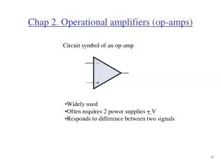
Chap 2. Operational amplifiers (op-amps). Circuit symbol of an op-amp. Widely used Often requires 2 power supplies + V Responds to difference between two signals. 2.2 Ideal op-amp. Characteristics of an ideal op-amp R in = infinity R out = 0

E N D
Chap 2. Operational amplifiers (op-amps) Circuit symbol of an op-amp • Widely used • Often requires 2 power supplies + V • Responds to difference between two signals
2.2 Ideal op-amp • Characteristics of an ideal op-amp • Rin = infinity • Rout = 0 • Avo = infinity (Avo is the open-loop gain, sometimes A or Av of the op-amp) • Bandwidth = infinity (amplifies all frequencies equally)
+ - Model of an ideal op-amp I+ V+ + I- Vout = A(V+ - V-) V- - • Usually used with feedback • Open-loop configuration not used much
Summary of op-amp behavior Vout = A(V+ - V-) Vout/A = V+ - V- Let A infinity then, V+ -V- 0
Summary of op-amp behavior V+ = V- I+ = I- = 0 Seems strange, but the input terminals to an op-amp act as a short and open at the same time
To analyze an op-amp circuit • Write node equations at + and - terminals (I+ = I- = 0) • Set V+ = V- • Solve for Vout
2.3 Inverting configuration Very popular circuit
Analysis of inverting configuration I2 I1 = (Vi - V- )/R1 I2 = (V-- Vo)/R2 set I1 = I2, (Vi - V-)/R1 = (V- - Vo)/R2 but V-= V+ = 0 Vi / R1 = -Vo / R2 Solve for Vo Vo / Vi = -R2 / R1 I1 Gain of circuit determined by external components
Rf R1 V1 V2 V3 R2 R3 2.4 Applications of the inverting configuration Current in R1, R2, and R3 add to current in Rf (V1 - V-)/R1 + (V2 - V-)/R2 + (V3 - V-)/R3 = (V- - Vo)/Rf Set V-= V+ = 0, V1/R1 + V2/R2 + V3/R3 = - Vo/Rf solve for Vo, Vo = -Rf(V1/R1 + V2/R2 + V3/R3) This circuit is called a weighted summer
Integrator(2.4 Applications of the inverting configuration) I2 I1 = (Vi - V-)/R1 I2 = C d(V- - Vo)/dt set I1 = I2, (Vi - V-)/R1 = C d(V- - Vo)/dt but V-= V+= 0 Vi/R1 = -C d(Vo)/dt Solve for Vo Vo = -(1/CR1)( Vi dt) I1 Output is the integral of input signal. CR1 is the time constant
Problem 2.28 Given an integrator with a time constant of 1mS, with a square wave input as shown below, find the output. Vo = -(1/CR1)( Vi dt) CR1 = 1mS, and Vi =1V for 0 < t < 0.5mS Vo = -(1/1mS)( dt), for 0 < t < 0.5mS Vo = -(t/1mS), for 0 < t < 0.5mS Vo = (t/1mS), for 0.5 < t < 1.0mS 1V t 0 0.5 1 1.5 mS -1V
Problem 2.28 1V Vo = -(t/1mS), for 0 < t < 0.5mS Vo = (t/1mS), for 0.5 < t < 1.0mS When t = 0.5mS, Vo = -0.5V t 0 0.5 1 mS CR1 = 1mS CR1 = 0.5mS -1V
Exercise 2.6 Design an integrator (find RC) such that the output has a 20Vp-p amplitude given the input below.(Find the RC time constant) Vo = -(1/CR)( Vi dt) Vi = 10V, 0 < t < 1.0mS Vo = -(1/RC) Vo = -10t/RC let t = 1.0mS, and Vo = -20 20 = 0.01/RC RC = 0.5mS Vi 10V t 2mS Vout -10V
I I Vi 2.5 Noninverting configuration (0 - V-)/R1 = (V- - Vo)/R2 But, Vi = V+= V-, ( - Vi)/R1 = (Vi - Vo)/R2 Solve for Vo, Vo = Vi(1+R2/R1)
Buffer amplifier Vi = V+ = V- = Vo Vo = Vi Isolates input from output
Analyzing op-amp circuits Write node equations using: V+ = V- I+ = I- = 0 Solve for Vout Usually easier, can solve most problems this way. Write node equations using: model, let A infinity Solve for Vout Works for every op-amp circuit. OR
Input resistance of noninverting amplifier Rin = Vin / I, from definition Rin = Vin / 0 Rin = infinity V- I Vout = A(V+ -V-) V+
Input resistance of inverting amplifier Rin = Vin / I, from definition I = (Vin - Vout)/R I = [Vin - A (V+ - V-)] / R But V+= 0 I = [Vin - A( -Vin)] / R Rin = VinR / [Vin (1+A)] As A approaches infinity, Rin = 0 I V- V+ Vout = A(V+ - V-)
Vi Summary of op-amp behavior Inverting configuration Noninverting configuration Vi Rin = 0 at this point Vo/Vi = 1+R2/R1 Rin = infinity Vo /Vi = - R2/R1 Rin = R1
Difference amplifier Use superposition, set V1 = 0, solve for Vo (noninverting amp) set V2 = 0, solve for Vo (inverting amp) Fig. 2.21 A difference amplifier.
Difference amplifier V2 R4/(R3+R4) Vo1 = -(R2/R1)V1 Vo2 = (1 + R2/R1) [R4/(R3+R4)] V2 Add the two results Vo = -(R2/R1)V1 + (1 + R2/R1) [R4/(R3+R4)] V2
Design of difference amplifiers Vo = -(R2/R1)V1 + (1 + R2/R1) [R4/(R3+R4)]V2 For Vo = V2 - V1 SetR2 = R1 = R, and set R3 = R4 = R For Vo = 3V2 - 2V1 Set R1 = R, R2 = 2R, then 3[R4/(R3+R4)] = 3 Set R3 = 0
Input resistance of difference amplifiers When measuring Rin at one input, ground all other inputs. Rin at V1 = R1, same as inverting amp Rin at V2 = R3 + R4
Improving the input resistance of amplifiers Add buffer amplifiers to the inputs Rin = infinity at both V1 and V2
Prob. 2.55 (a) Find Rin at V1. Ground V2, Rin = R. (b) Find Rin at V2. Ground V1, Rin = 2R. I + V - (c) Find Rin between V1 and V2. Rin = V/I from definition. Write voltage loop, V = IR + IR, I = V/2R Rin = V/I = V2R/V Rin = 2R I
Prob. 2.55 (d) Find Rin between V1 and V2 connected together and ground. I2 I + V - Rin = V/I from definition I1 = V/2R from Ohm’s law I2 = (V - V/2)R = V/2R because V+= V- Rin = V/ (I1 +I2) = V2R/2V Rin = R I1 = V/2R V/2
- - Vout = A(V+ - V-) Vout = A(V+ - V-) C + + + + - - 2.7 Frequency response of op-amps Model of an op-amp with frequency response Model of an ideal op-amp We assume low-pass filter behavior
Magnitude response of single capacitor circuit 20 log|A| where w0 = 1/RC Fig.1.23(a) Magnitude response of (single time constant) STC networks of the low-pass type.
Open-loop frequency response of op-amp Open-loop gain at low frequencies Break frequency(bandwidth), occurs where Ao drops 3dB below maximum Unity gain frequency, occurs where Ao = 1 (A = 0dB)
Gain-bandwidth product For any op-amp circuit without external capacitors: ft = |A| fb A = voltage gain of circuit fb = break frequency ft = unity gain frequency, fixed!
Frequency response of op-amp ft = |A| fb 1MHz = (10 000) 100Hz 1MHz = (1000) 1KHz 1MHz = (10) 100KHz Tradeoff between gain and bandwidth ft = 1MHz
Example Given A = 1 000 000 at low frequencies, at 10kHz A = 100, and ft = 1MHz, find A at 1kHz. Find break frequency ft = A fb fb = ft / A = 1MHz/1M fb = 1 A = 1 000 000 = 120 dB Because 1kHz > fb, A = 20dB greater gain than at 10kHz. A = 100 = 40 dB
Example Given A = 106 dB at DC, ft = 2MHz, find A at f = 2kHz, 20kHz, and 200kHz. ft = A fb fb = ft / A = 2MHz/200 000 fb = 10 A = 106 dB (200 000) A at 2kHz = 60 dB A at 20kHz = 40 dB A at 200kHz = 20 dB ft = 2MHz
Problem 2.69 Given an inverting amp circuit with A = -20, Ao of op-amp at low frequencies = 10 000, ft = 1MHz. (b) find A at 0.1 fb. For f < fb, A = A of circuit = -20 = 26dB. (c) find A at 10 fb. For f > fb, A = A of circuit - 20 dB, A = 26 dB - 20 dB = 6dB (a) find fb, fb = ft / A fb = 1MHz / |20| fb = 50kHz
Problem 2.74 Design an circuit for A = 100 at 5MHz using op-amps with ft = 40MHz. --------- For fb = 5MHz, A = ft / fb = 8. This is the maximum gain of the op-amp! Cannot meet the specifications unless we use multiple op-amps with lower gains. If A = 100, use A = A1 A2 A3 = 5 x 5 x 4. The bandwidth is now fb = ft / A = 8 MHz. R2 = 4KW R1 = 1KW A1 = 5 R2 = 5KW R1 = 1KW A2 = - 5 R2 = 4KW R1 = 1KW A2 = - 4
Frequency response of op-amp circuits • Open-loop op-amp • Inverting and noninverting amplifiers • Low-pass filter • High-pass filter
Frequency response of open-loop op-amp Open-loop op-amp: ft = Ao fb where Ao is gain of op-amp
Constant Gain-Bandwidth product of op-amp ft = |A| fb 1MHz = (10 000) 100Hz 1MHz = (1000) 1KHz 1MHz = (10) 100KHz Tradeoff between gain and bandwidth ft = 1MHz
Frequency response of inverting and noninverting amplifiers Inverting or noninverting amplifier: ft = |A| fb,where A = gain of circuit Vi A = - R2 / R1, inverting A = 1 + R2/R1, noninverting - 20 dB/decade |A| fb ft
C Vi Frequency response of low-pass filter A = - Z2 / Z1 Z2 Z1 • At large frequencies A becomes zero. • Passes only low frequencies.
C Vi Frequency response of low-pass filter Low-pass filter: C acts as a short at high frequencies, gain drops to zero at high frequencies, ft |A| fb.fb = 1/2pR2C Due to external capacitor Due to op-amp - 20 dB/decade fb
C Vi Frequency response of high-pass filter A = - Z2 / Z1 Z2 Z1 • At large frequencies A becomes - R2 / R1. • Passes only high frequencies.
C Vi Frequency response of high-pass filter High-pass filter: C acts as an open at low frequencies, gain is zero at low frequencies, Due to external capacitor Due to op-amp fL = 1/2pR1C bandwidth
C Vi Design of a high-pass filter Design the circuit to obtain: High-frequency Rin = 1KW High-frequency gain = 40dB lower 3 dB frequency = 100Hz • Rin = R1 + 1/sC. At high frequencies, s becomes large, Rin R1. Let R1 = 1KW • A = - R2 / (R1 + 1/sC). At high frequencies, s becomes large, A - R2 / R1 . • A = 40dB = 100, 100 = R2 / 1KW, R2 = 100KW. • fL = 1/2pR1C C = 1/2p R1 fL, C = 1/2p(1KW)100 = 1.59mF
Design of a high-pass filter 20 dB/decade (due to capacitor) -20 dB/decade (due to op-amp) fL = 100Hz
C2 C1 Vi Bandpass filter • Both C2 and C1 act as shorts at high frequencies. • C2 limits high-frequency gain • C1 limits low-frequency gain • The gain at midrange frequencies = - R2 / R1 • fL = 1/2pR1 C1 • fH = 1/2pR2 C2 20 dB/decade (due to C1) -20 dB/decade (due to C2) bandwidth fL fH
2.8 Large-signal operation of op-amps • Saturation • Input must be small enough so the output remains less than the • supply voltage. • Slew rate • Maximum slope of output voltage. Response time of op-amps are • described by a slew rate rather than a delay.