Download
1 / 5
50 likes | 175 Vues
This review delves into the FTK Rear Transition Card used at the University of Chicago, providing a comprehensive overview of its design, capabilities, and power consumption. The card features multiple I/O options including QSFP and SFP connectors, optimized routing for High-Speed and LVTTL lines, and a careful selection of materials to minimize signal loss. With specific power consumption estimates, it is estimated that the card draws between 70-75 W, addressing the needs of four processor FPGAs and input FPGAs, making it a vital component in high-performance computing systems.

E N D
FTK Rear Transition Card Board Review Mircea Bogdan The University of Chicago March 12, 2013
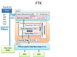
FTK Rear Transition Card Block Diagram • 9U VME Rear Transition Card • I/Os: • 2 x QSFP (8 x RxTx @ 6Gbps) • 1 x SFP (1 x RxTx @ 2Gbps) • P3 Connector: - 12 x Out @ 2Gbps • 16 x In @ 2Gbps • P2 Connector: • - VME: Data, Addr, Aux • - HOLDs to Input FPGAs (4+8) • - HOLDs from Processor FPGAs (4x4) • - FREEZE In, Out
FTK Rear Transition Card Power Supply Issues • Power Requirement Estimate (4 Processor FPGAs, 4 RLDRAMs, 2 Input FPGAs): • Power consumption per Processor FPGA ~ 12W • Power consumption per Input FPGA ~ 3 W • Total Power Consumption Estimate ~ 70-75 W per card Supply Options per Slot (Front Modules DO NOT draw any +5V current): P2/P0: +5V rated for 18.5/11.5A (20C/70C), total: 57.5W to 92.5W. P0: Vw, Vx, Vy, Vz: at +5V rated each for 4A/3A (20C/70C), total: 60W to 80W. Option 1 and 2 combined: total: 117.5W to 172.5W. P0: Vw, Vx, Vy, Vz: at +15V rated each for 4A/3A (20C/70C), i.e. 180W to 240W total.
FTK Rear Transition Card Routing: - HS lines:- routed between ground planes, 6mil width, 4 mil gap, 100Ohm, reduced number of vias, ground return vias, first plane cut-out under AC caps, matched length in pair. - LVTTL lines: separate layers, 4 mil width, 50Ohm. - 2 Oz Copper on 1.1V POWER_1.
FTK Rear Transition Card Material Selection Attenuation = 2.3 f (tand) sqrt(er) Max trace length: 16” for 2Gbps, 4” for 6Gbps Note: The first AUX Test Card, made with FR4, has max trace length 12” for 2Gbps: Signal Loss = 1.6dB.