Download
1 / 9
90 likes | 264 Vues
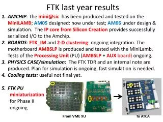
FTK Rear Transition Module. Board Review. Mircea Bogdan The University of Chicago November 11, 2014. FTK Rear Transition Module. 9U VME Rear Transition Module I/ Os : 2 x QSFP (8 x RxTx @ 6Gbps) 1 x SFP (1 x RxTx @ 6Gbps ) P3 Connector: - 12 x Out @ 2Gbps 16 x In @ 2Gbps

E N D
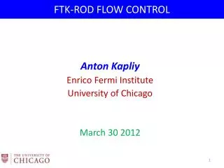
FTK Rear Transition Module Board Review Mircea Bogdan The University of Chicago November 11, 2014
FTK Rear Transition Module • 9U VME Rear Transition Module • I/Os: • 2 x QSFP (8 x RxTx @ 6Gbps) • 1 x SFP (1 x RxTx @ 6Gbps) • P3 Connector: - 12 x Out @ 2Gbps • 16 x In @ 2Gbps • P2 Connector: • - VME: Data, Addr, Aux • - HOLDs to Input FPGAs (4+8) • - HOLDs from Processor FPGAs (4x4) • - FREEZE In, Out Prototype Rev. B – 3 pieces finished 7/15/2014
FTK Rear Transition Module -VME Block Diagram for a typical VME Slave Module Interface. The Rear Transition Module (RTM) receives power from the crate, but is not part of the VME data transfer bus. Generally, the RTMs can not be accessed via the Crate CPU, and are used only to bring IO to the front processing module.
FTK Rear Transition Module -VME Data Communication Structure for the FTK VME Rear Transition Module. The method employs the J2, user-defined, feed-through pins to communicate with the corresponding front module, and extend its local data, address, and control buses to the rear. Method for backplane data communication with the VME Rear Transition Modules developed for the ATLAS FTK Project, Bogdan, M.,;Magalotti, D. ;Piendibene, M. ; Shochet, M. ; Tompkins, L.A.; (NSS/MIC), 2013 IEEE Oct. 27 2013-Nov. 2 2013, ISBN: 978-1-4799-0533-1
FTK Rear Transition Module - Power • Power Requirement Estimated in 2013 for 200MHz clock, and 12V supply: 75W per Module. • Power Consumption Measured on prototypes with 48V power supply: • 51W at 50MHz clock; • 54W at 100MHz clock; • 64W at 200MHz clock (firmware not final). Power Supply Voltage Requirements: P0: Vw, Vx, Vy, Vz: +48V (38-55V), and P2: +5V/100mA For production, we will eliminate the need for the +5V supply by adding one LDO to the board. Other Power Supply Options (+5V or +12V) by changing wire jumpers and local fuses.
FTK Rear Transition Module - PCB • HS lines routed separately, between ground planes, 6mil width, 4 mil gap, 100Ohm, reduced number of vias, ground return vias, first plane cut-out under AC caps, matched length in pair +/- 1ps. • Minimized sensitivity to laminate weave skew variation: • Nelco400-13EPSI has reduced sensitivity; • Wider traces (6 mils) have reduced sensitivity; • Minimize orthogonal trace routing and route in short segments; • Future PCBs at an angle of 22.5 degrees to the weave of substrate. • All HS lines were tested at for BER = 10-15 on prototype Rev. B.
FTK Rear Transition Module Rev. A to Rev. B Changes • Prototype Rev. A (2 pieces finished in 2013): • Missing 1 REF resistors for each FPGAs (fixed with “blue wires”); • One FPGA got damaged (ESD?) and was replaced (got ESD Survey and implemented ESD Control Program for our shop) • Intermittent FPGA configuration issues (fixed in Rev.B by improving JTAG chain integrity); • 48V Power Option required because of power needs of other boards in the crate (feature added with “blue wires”). • Prototype Rev. B (3 pieces finished in July 2014): • All “blue wire” fixes were included in Rev. B. design, and are working fine; • Intermittent FPGA configuration issues were addressed, and don’t exist any more • In total, about 100 configurations performed on Rev. B boards with no error; • Included new Power Sequencing Circuit (as required by FPGA Data Sheet); • sequence timing was measured on one Rev. B module. • The Rev. B modules are working as specified.
FTK Rear Transition Module To Do before Production • Minor PCB changes required before production: • Add one TO220 LDO to eliminate the need for the 5V supply (module will run on 48V alone); • Change one trace width on the Top Layer (will improve one 3.3V local supply); • Production plans: • We will have two 9U VME Crates in an ESD controlled environment; • We will have two Front Test Modules and one production AM Board in our test stand. • We will require Flying Probe test to be performed by the manufacturer (We had one bad resistor installed on one of the Rev. B modules, and this test will catch errors like that.)
FTK Rear Transition Module – Docs • Schematics http://edg.uchicago.edu/~bogdan/FTK_Rear_Transition_Module/schematicsB.html • Layout http://edg.uchicago.edu/~bogdan/FTK_Rear_Transition_Module/layoutB.html • Notes: • The Schematics page has links to all schematics; • The Layout page has links to the specification drawing, assembly drawings, neutral file, net lengths file, Gerber files, plots of Gerber files, BOM file with manufacturing instructions.