Download
1 / 43
430 likes | 523 Vues
Explore the machine and detector upgrade plans, module integration, sensor technology, readout architecture, and challenges faced by the upgrade community at SLHC. Learn about the powering schemes, service constraints, and more.

E N D
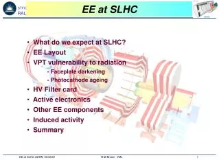
Requirements of the ATLAS Strips at SLHC Didier Ferrère, DPNC Université de Genève In behalf of the ATLAS Upgrade community ACES09, 3-4 March 2009 at CERN • Outlines: • Machine and detector upgrade plans • Layout and challenges • Module integration • Silicon sensors & FE readout • Powering schemes • Readout architecture overview • Service constrains • Summary
Machine Scenario Parameters SLHC – Phase II Scenario 1 Scenario 2 Bunch spacing [ns] 50 25 Proton/bunch Nb[1011] 4.9 1.7 b* at IP1&5 [m] 0.25 0.08 shutdowns Longitudinal profile Flat Gaussian Rms bunch length sz[cm] 11.8 7.55 Peak luminosity [1034 cm-2s-1] 10.7 15.5 Effective luminosity (5h) [1034 cm-2s-1] 3.5 3.6 Peak events per crossing 403 294 Expected shutdowns: - 6 to 8 months in 2012 - 18 months in 2016 B-Layer replacement Detector Upgrade Time shifted by 1 year! ACES09, D. Ferrère 2
Detector Upgrade Plan • Current ID is designed to survive ~600fb-1 integrated luminosity expected for 2016 • New ID is therefore planned for installation/operation in 2018 with a higher yearly integrated luminosity of 600fb-1 • Many challenges and critical issues: Under investigation for most of them • Schedule: • - End of 2009: Letter Of Intend • - 2010: Technical Proposal • - 2011: Costing and MOU by April and TDR by December • - 2012: PRRs • - 2017: Installation at the end of the year • Upgrade organization: Executive bodies, Steering Group, Technical Coordination, Project Office and Working groups The Upgrade community has to keep in mind the detector challenges at SLHC… ACES09, D. Ferrère 3
Challenges High speed Serializer Optical links DCS Layout Trigger Tracking Performance ACES09, D. Ferrère 4
Detector Upgrade Issues Topics under investigation for the tracker upgrade: • New ID layout: Only silicon pixel and strip detectors Simulations • Trigger: Need to workout on a TDAQ/Detector interface specification • New detector technology: n-in-p planar for strips • New ASICs technologies: Deep submicron 250 nm 130nm or 90 nm • Cooling with more headroom: Silicon temperature below -20°C • New powering scheme: Serial powering or DC-DC for parallel powering • Faster readout: FE asics (160/320 Mbps) and optical link (5Gb/s) SCT 1.3 kch/link Upgrade 123 kch/link • Module integration will be grouped on a stave or a super-module structure performances • DCS is proposed to be partially integrated into the readout architecture • Engineering: - Assemble and commission the complete ID in a surface building - Service reuse of cables between counting room and detector • Installation: Limited access time inside the cavern ACES09, D. Ferrère 5
Strip Detector Today SCT EC at SR1 ~60 m2 of silicon installed today 16 years from LOI to readiness! SCT barrel integration Wire bonding ACES09, D. Ferrère 6
ID Upgrade Layout - 2.6% - 1.8% - 1.0% Short and Long Strip Occupancy (400/BCO) Simulation G3, G4 should drive the layout: - Reasonably low occupancy - Good tracking efficiency, low fake rate 6 months Layout TF led by L. Rossi Including disks this leads to: Pixels: 5 m2, ~300,000,000 channels Short strips: 60 m2, ~30,000,000 channels Long strips: 100m2, ~15,000,000 channels Evolution of Strawman Layout since 2006 Fixed length barrel Stawman08 2 layers - 3 layers - 4 layers - Strawman06 ACES09, D. Ferrère 7
Radiation Background in ID at SLHC Simulation using FLUKA2006 Issues • Thermal management and shot noise. Silicon looks to need to be at less than -20oC (Thermal runaway). Si power: 1W @ -20°C 4W @ -10°C 10W @ 0°C High levels of activation will require careful consideration for access and maintenance. 1 MeV equivalent neutron fluences assuming an integrated luminosity of 3000fb-1 and 5cm of moderator lining the calorimeters (reduces fluences by ~25%) With safety factor of 2 Si-strip has to withstand 9.1014neq/cm2 ACES09, D. Ferrère 8
Silicon Sensors Hamamatsu ATLAS07 4 short strips: ~2.3 cm 20 mrad on 1side Straight on the other side New trackers required to survive 6000fb-1 ie short strip detectors to withstand 9×10¹⁴neq/cm2 at 500V With 750e- noise, → S/N ≈12-15 (0.9mA/strip @ -15°C) ACES09, D. Ferrère 9
Module Integration Module #1 Module #2 Module #12 Cooling In TTC, Data & DCS fibers Opto SC DCS interlock DCS env. IN Cooling Out SMC Hybrid Service bus PS cable ~1.2m MC MC MC MC MC MC • Key features: • Integrates all the functionalities and the requirements like: Sensor, FE, service bus, powering, DCS, cooling, mechanical precision and stability, controller cards, optical readout link, connectors and fittings… • Low material budget with design and technology optimization • Precision: built-in accuracy and mechanical stability • Thermal management is critical to prevent runaway on the silicon • cooling, design, material and performance to be optimized • Manufacturability, yield and cost ACES09, D. Ferrère 10
Module Integration - Stave Carbon fiber facing Bus cable Power, DCS, HV Carbon honeycomb or foam Hybrids Readout IC’s Coolant tube structure Sensor From A. Greenall Bus cable 100mm TTC (multi drop LVDS) - Digital I/O Short Strip Double-sided Stave - Baseline 1st prototype module from Liverpool ACES09, D. Ferrère 11
Double-sided Module - Backup Lateral insertion (KEK) End insertion (Geneva) ACES09, D. Ferrère 12
Endcap Petals Petal layout Serial Powering Lines Mechanical prototype • Endcap strip: • 5 discs on each side • 32 petals/disc • ➔ 4 different petals (325mm<R<950mm) • 6 different detector types mounted on petals • ➔ Max 18 sensors/petal • ➔ Min. 12 sensors/ petal • 8 hybrid types • Issues: Layout, modularity, powering… C. Lacasta IFIC ACES09, D. Ferrère 13
Readout Electronics - IC • CMOS [130nm or 90nm] is the commercial technology choice for the Upgrade: • Known for the radiation hardness (Transistors with GAA) • Good for large volume production • Good for low power consumption Current Asics program Strip: ABCN 250nm 130nm @ 160/320 MHz • Issues: • Technology choice for a production in > 3 years: 130nm, 90nm? • Number of channels per FEIC is left opened so far: More than 128 may have some advantages • Power consumption (Strips): • - 250nm (ABCN) Measured 3.6 mW/ch @ 40MHz • - 130nm Max target 1 mW/ch @ 160MHz (expected 0.5-0.6 mW/ch) • Single Event Upset (SEU): 130 nm technology seems to be 10 times more sensitive than 250 nm • Need to consider new readout protocol • Design prototype and tests manufacturability on a fixed timescale • Design and tools of 130nm or 90nm are more complex ACES09, D. Ferrère 14
FE - ABCN Digital part : reuse of existing SCT protocols, SEU protections, 80Mbits/sec output rate, power control , 2mW/channel @2.5V 128 Channels Front-End opt. for Short Strips 0.7mW/channel ABCN 250nm is an intermediate version of the FE chip for modules prototypes developments F. Anghinolfi Serial regulator to provide analogue from a unique digital+ analogue power source Shunt regulators (2 options) to exercise 2 different serial powering systems ACES09, D. Ferrère 15
ABCN in 250nm Gradually increased the # chips Subset of a result of a 20 chip ABCN Liverpool hybrid • ABCN program: • Test and validate the current chips in 250nm technology • Use those chips for prototypes • Work on the final choice technology • Good progress so far in testing: • - Digital and analog performance as expected • - No malfunctioning found • - Yield seems good • Functionality and performances to be tested @80MHz • Wafer screening under investigation Noise as expected ~380e ACES09, D. Ferrère 16
Silicon with ABCN-250nm Divided first ABCN into three sections connected to 2.5 cm, 5 cm, 7.5 cm silicon strips -Operating point Noise prediction from J. Kaplon with no detector leakage ACES09, D. Ferrère 17
Module Controller (MCC) From M. Newcomer • Features: • Single Point interface between hybrid FEIC’s and Stave distribution of TTC and ROD read out signals. • DCS Monitoring • Power Management ?? • Short and long strip readout clock: 160 and 80 MHz respectively SC MCCL1, BC, CMDBussed to all MCC For the Serial Power (SP) option the MCC needs AC coupled receivers. SC MCC Hybrid DataDirect Link / MCC For the SP option the Stave Controller needs AC coupled receivers. Stave Bus MCC FEICL1, BC, DC, CMD Bussed to FEIC’s MCC FEIC FEIC Data @128ch/FEIC Multiple Loop Bi-directional Serial. @512ch/FEIC Dedicated Lines to MCC ?? Hybrid Bus ACES09, D. Ferrère 18
Powering 24i i ID Upgrade has a lot of more channels to power than current ID 2 options are considered: - Serial powering - DC-DC conversion ABC-Next 250 nm : Vcc = 2.2 V, Icc = 0.036 A Vdd = 2.5 V, Idd = 0.12 A 0.38W/FE 30.4W/module 365W/stave IP ABC-Next 130 nm : 1mW/ch expected 0.13W/FE 10.2W/module 123W/stave SP IP ~2 order of magnitude higher of line width than SP or DC-DC DC-DC • Issues: • DC-DC:EMI (switching noise); radiation-hardness; high gain/efficiency • Serial Powering: System aspect, Optimize protection/by-pass circuitry, Evaluate custom circuitry and identify best architecture • System:Work out cable budget; LV & HV distribution, schedule… ACES09, D. Ferrère 19
Serial Powering Tested so far: 1) Pixel stave with FE-I3 (old, published) 2) 6 SCT modules in series with ABCD 3) 6 module stave with ABCD 4) 30 module stave test vehicle and stave Electrical performance is excellent in all tests. Multi-drop AC- LVDS coupling works • On work: • Several options are considered: Shunt integrated in the FE, Shunt outside and transistor in the FE, Shunt and transistor outside FE • Overvoltage protection and enable scheme to be worked-out and tested Tested with ABCN and SPi 4 V x 30 hybrids = 120 V (0.8 A) Strip Stave from LBNL In future: 1.5V X 20 hybrids = 30 V ACES09, D. Ferrère 20
DC-DC Powering 2 Converter stage2 on-chip Detector Hybrid controller 2.5V bus 1.8V bus 10-12V 2 Converter stage 1 Key features: Efficiency, modularity, flexibility Work development common at CERN for ATLAS and CMS From F. Faccio Voltage for SMC and optoelectronics generated locally by a converter stage 1 Stave Only 1 power line/stave 10-12V • Distribution with 2 conversion stages • Stage 1: • 2 converters: 2.5V analog and 1.8V digital • Higher efficiency if more hybrid powered • Integrated into a modular circuit board • Stage 2: • Directly integrated into the FE asics • Switched capacitor converter with fixed conversion ratio = 2 • 2 converters one for analog and one for digital ACES09, D. Ferrère 21
Readout Architecture IO for slow control IO for slow control (power, temp...) (power, temp...) GBT could be a good candidate IO for slow control (power, temp...) FE Chip FEIC x10-20 /MC TTC N Links Data Module Controller TTC Electrical LVDS Electrical LVDS Data MC x24 /SC M Links Stave Optical links TTC Controller • Difference with current SCT architecture: • MC and SC stages • FE Data at 160-320 instead of 40 Mbps • Data to off-detector will transit via high speed links • Short-strip stave bandwidth 3.84 Gbps Max needed for strip project • Top and bottom side readout are decoupled • DCS diagnostics data possibly integrated into the readout chain • FE redundancy scheme is differently implemented (No bypass) • Readout protocol has to be different (avoid token, data coding,…) Data SC x2 /stave ACES09, D. Ferrère 22
Optical Transmission Data out 1 Data out 2 BOC ROD Opto Devices Data out 3 GBT Data out n 160-320 Mbps 5 Gbps Work focus on high speed data link @ 5Gbps to minimize the number of fibers The data transmission will be done for half stave (Strip) 5 Gbps 10 Gbps • Challenges and investigations: • Opto-devices not enough radiation hard for the pixel region BUT OK for strips • Radiation harness of all the components especially at low temperature -20°C • Bit Error Rate (BER) versus SEU Error correction mandatory at sLHC • Wavelength study: 850nm versus 1310 nm (more radiation hard) • 1310 SM VCSELs becoming available now which are being investigated • Versatile link working group well structure (common to ATLAS and CMS) ACES09, D. Ferrère 23
Possible Requirements Dead time versus buffer depth From Tony Weidberg Here occupancy increased by a factor of 1.7 for a dead time of 1% • - Trigger Rate <L1> = 100 kHz • - Assume 20 MHz BC <pile up> = 400 • 256 channels/FEIC • Readout through 1 MCC • Look at short strip detector only (worst case) • Redundancy scheme to be considered at all the stages of the readout chain from FEIC to SC and Opto-electronics • Readout protocol and the data format has to cope with high speed readout, the easiness and the occupancy • SEU robustness is essential Replica logic has to be integrated where it is necessary • Need at maximum an effective data rate of 3.84 Gbps at the optical interface (short-strip stave) • An error correction scheme should be necessary due to BER in the optical interfaces ACES09, D. Ferrère 24
DCS Architecture • Mainly 2 options proposed so far: • Option 1: - All the Hybrid and FE chip DCS info are readout via Fiber • - One hybrid temp per stave is independently readout • Option 2: Same as option 1 except that all the hybrid temperatures are readout independently via an independent DCS chip NB: In all options interlock based on NTC cooling loop, Environmental, SMC temp are separated from data readout ACES09, D. Ferrère 25
DCS versus Operation On request DCS Cooling Survey Pre-operation SMC ramp & Opto com Module ramp Operation Detector Cold Cooling Interlock Active, Env. data accessible, PS Low data volume Up to 5x10⁴ data/day/stave @ 0.1Hz Module Interlock Active, Module temp, local PS accessible Medium data volume Up to 4.3x10⁵ data/day/stave @ 0.1Hz From DCS system with option 2 From DAQ with option 1&3 FE DCS, Hybrid power accessible High data volume Max 9x10⁶ data/day/stave @ 0.1Hz Time ACES09, D. Ferrère 26
Services • Electrical service available: • SCT: - 4088 cables (LV, HV) • - 144 fiber ribbons • Pixel: - 1808 cables (LV, HV) • - 84 fiber ribbons • TRT: - 40128 cables (LV, HV, signal) NB: Fibers have to be reinstalled to suit with bandwidth of ~5Gbps PP1 concept - N. Massol It is where there is a lot of constrains! • Constrains: • Low mass inside the ID volume required • Connection to the ID flanges should be fast and reliable (Limited access due to radioactivity level) • Have to deal with the existing cables from counting rooms to PP2 • It has been excluded to reuse all the services at the various PP1 position • For cooling pipes the cooling choice will strongly define what to do and the possible recycling ACES09, D. Ferrère 27
Conclusions • 3 ID Strawman layout versions have been investigated but a new baseline is expected in fall and to be presented at the LOI (early in 2010) • Need also to deal with the possibility of a change in the layout with a track trigger Implication on the readout architecture? • The strip community are investigating the short (2.5cm) and the long strips (10 cm) for barrel and EC with stave or petal concept • A strip readout Task Force has been initiated and is led by P. Farthouat. Specifications for the complete readout chain has to come soon to progress • Interim document “Architecture of the Readout Electronics” • So far ABCN in 250nm is working well and the noise performance is as expected • Many interleave fields: powering, readout, opto-electronics, DCS, services • Prototyping is vital and all the future new ICs have to be tested on a real size stave/petal object • Schedule is tight for a TDR in 2011 • Need soon to freeze the FE technology, the readout protocol, the powering scheme and the DCS options. ACES09, D. Ferrère 28
Backup Slides ACES09, D. Ferrère 29
Backup Slides 2 x 10 128 channels SHORT STRIPS 5 times 512 channels Module arrangement, Short strips, 512 channels ABCN Module arrangement, Short strips, 128 channels ABCN ACES09, D. Ferrère 30
128 ch FEIC layout Variations on channel number Area for pads, power circuits etc RAMFF cells RAMSR cells FE pads 2 rows 500um x 0.8cm 128x128 Main pipeline Main pipeline 128x256 128x128 128x128 Main pipeline FE channels 128 1mm x 0.8cm 128x128 RO Buffer 0.8cm RO Buffer 3.83mm Digital area 630um x 4mm Pipeline/RAM REAL area From 130 nm Artisan Library (2 options) 50K cells 50K cells Chip size estimate for 130nm IBM CMOS tech. 128 channels 50K cells as ABCN design, at average density (150Kcells/mm2) 4mm 630um ACES09, D. Ferrère 31
512 ch FEIC layout ABCN : NEXT STEPS 512 channels chip option, Short strips RAMFF cells RAMSR cells One digital block, processes 128 channels FE pads 4 rows 700um x 1.8cm 128x128 Main pipeline Main pipeline 128x256 128x128 128x128 Main pipeline FE channels 512 1mm x 1.8cm 128x128 RO Buffer RO Buffer Max digital area 630um x 1.6cm 50K cells 50K cells Digital arrangement in 4 identical blocks, each one for 128 channels 4mm 1.8cm 630um 3.83mm ACES09, D. Ferrère 32
Interim Report ACES09, D. Ferrère 33
Upgrade Bunch Pattern nominal 25 ns ultimate & 25-ns upgrade (ES, FCC, & LE) 25 ns 50-ns upgrade (LPA), no collisions in LHCb! 50 ns 50-ns upgrade with 25-ns collisions in LHCb 50 ns 25 ns ACES09, D. Ferrère 34
Backup Slides Average luminosity ACES09, D. Ferrère 35
Thermal Runaway Tmax (FE)= -19.4°C Cooling @ -30°C with CO2 Tmax (Si)= -20.7°C sLHC Uncontrolled Tgas has a significant impact on Si-temperature and on the runaway! ACES09, D. Ferrère 36
Readout Scheme - Redundancy Normal readout – 2 rows of 10 chips MC 1 dead chip – 2 asymmetrical rows MC 160 Mbits/s 160 Mbits/s X 10 FEICs 10 FEICs MC MC Path Normal data flow: each 160 - Mbits/s link One failing FEIC: one of the 160 - Mbits/s link reads out 10 FEICs Is reading - out more than 10 FEICs Data alt alt MC MC Unused Extra Data Path 10 FEICs 320 Mbits/s for reverse direction 10 FEICs - 320 Mbits/s - 160 160 160 Mbits/s 160 Mbits/s To To SMC SMC • Other stages of the readout chain: • MC: 2 chips are installed per hybrid and 100% fail safe scheme can be adopted • SMC: Similar scheme as MC could be specified • Opto: To be defined – One option could be to link the TTC and the data with the SMC of the other side of the stave Bandwidth? ACES09, D. Ferrère 37
Readout Protocol command lvds rcv lvds drv logic in logic out L1 L1 L1 L1 D D Q Q led_out data data data FIFO FIFO FIFO FIFO FEI FEI M CC S S E MCC Xon/off Xon/off Xon/off CK CK 160MHz 160MHz Option 1 Token mechanism currently used with ABCD and ABCN tline tsetup thold tout tin tdrv trcv chipA chipB NB: At 160Mbps: 2.8ns remains to tout and tin… Not enough for any logic @ 250nm! Option 2 Word enable via Xon/Xoff line(s) No synchro. NB: Data are pushed from left to right into the FIFO. Xoff is up when the FIFO is full! Option 3 - No synchro - Robust if dead FEI Star configuration – Data concatenation into MCC ACES09, D. Ferrère 38
Readout Protocol – Data Packets Fixed sized data packet Header Data Header Data Header Data Next chip 1 chip Still to be defined: How to encode the data and bandwidth expectation? {Header}{+ L1_ID}{+ BC_ID}{MC_ID}{+ Chip_ID}{ + CH_ID + Data}{+ Trailer} … {+ Reg_ID +Data} … … {+ ErrorCode} … DCS Data packet options for all chips: gap Fixed sized word packet Header W1 W2 W3 Trailer Header W1 W2 Trailer 1 chip Next chip gap Variable sized data packet Header Data Trailer Header Data Trailer 1 chip Next chip Works better with 256 ch/FEIC versus occupancy ACES09, D. Ferrère 39
SEU & BER Absolute requirement is to prevent the readout chain against off-state due to SEU Smooth run & operation • 130 nm technology has higher SEU cross-section due to smaller geometry and smaller digital voltage • Need to implement replica logic (triple vote logic) to increase SEU tolerances • Replica logics consume 3 times more space and therefore has to be used where it is absolutely necessary • P-I-N diodes and BER versus SEU has been studied by Versatile link teams Measurements obtained with a test system at PSI Work of Versatile Link group ACES09, D. Ferrère 40
Cooling One of the keys in the operational success! • Issues: • Define the fluid coolant: CO2 versus C3F8 • Service reuse and segmentation • Manifolding and impact on the system • Module design is directly dependent of the cooling choice • Requirements and specifications to be well defined and written-up • Known: • C3F8: We learnt a lot and still may be a lot to learn in long term operation! • Already a plant running BUT would it still be satisfactory in 10 years • Need to improve the pressure drop in the exhaust to allow a temperature close to -30°C. • CO2: LHCb, AMS have it! Looks good but not easily scalable to ID Upgrade but fine for IBL! • Less material for pipes, fittings and manifolds inside the ID volume • More safety margin for Si temperature. ACES09, D. Ferrère 41
Integration Baseline: - Integration of a 7 m long ID on the surface - Room for insertable/removable b-layer • Issues: • Layout not defined yet Engineering is based on 1 layout (not optimized) • Analysis (FEM) and dimensioning of main structural elements • Critical points under investigation: • Service space inside the ID volume critical between EC and Barrel strips and in the flange region • End of barrel strip where SMC and dense service region is expected • Cooling distribution and manifolds • Thermal management OC and Poly-moderator • Pixel optoboards position • PPF1 connection area and arrangement ACES09, D. Ferrère 42
Radiation Level Issue:Requirements to reuse much of ATLAS and the levels of activation anticipated: greatly complicate installation Minimize the tasks 1 week for catA (<6mSv/y) 2.5 weeks for catB (<15mSv/y) ACES09, D. Ferrère 43