Download
1 / 17
170 likes | 355 Vues
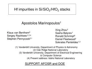
Hf impurities in Si/SiO 2 /HfO 2 stacks. Apostolos Marinopoulos 1. Xing Zhou 3 Sasha Batyrev 1 Ronald Schrimpf 3 Daniel Fleetwood 3 Sokrates Pantelides 1,2. Klaus van Benthem 2 Sergey Rashkeev 1,2,4 Stephen Pennycook 2,1.

E N D
Hf impurities in Si/SiO2/HfO2 stacks Apostolos Marinopoulos1 Xing Zhou3Sasha Batyrev1Ronald Schrimpf3Daniel Fleetwood3Sokrates Pantelides1,2 Klaus van Benthem2Sergey Rashkeev1,2,4Stephen Pennycook2,1 (1) Vanderbilt University, Department of Physics & Astronomy(2) Oak Ridge National Laboratory(3) Vanderbilt University, Department of Electrical Engineering & Computer Science (4) Present address: Idaho National Laboratory SUPPORT: AFOSR and DOE
0.8 nm • Stray Hf atoms in SiO2 interlayer (Oak Ridge National Lab) SiO2 HfO2 Silicon SiO2 interlayer formation during post-deposition annealing Hf atoms inside SiO2 (van Benthem and Pennycook) • Electrical measurements under switched-bias annealing • after irradiation and constant-voltage stress (Vanderbilt)
Constant-voltage stress (CVS) and irradiation (10 keV X-rays) applied to Si/SiOxNy/HfO2 stacks @ 25o – 150o C Pb centers H+ reactions at near-interface region Oscillations of interface-trap density by switching bias (Zhou, Schrimpf, Fleetwood)
interface 2 Å 4 Å 1 nm distance (Å) Number of Hf atoms versus distance from interface Single Hf atoms inside SiO2 interlayer
perfect structure substitutional Hf: localized perturbation E(int) = E(sub) + 4 eV interstitial Hf rebonding HIGH-ENERGY STATES !
SUBSTITUTIONAL IMPURITIES 1.4 eV penaltyfor segregation
Tu & Tersoff 2000 No particular crystalline polymorph quartz Hf atoms: markers Ordering of Si planes
Constant-voltage stress (CVS) and irradiation (10 keV X-rays) applied to Si/SiOxNy/HfO2 stacks @ 25o – 150o C Pb centers H+ reactions at near-interface region Oscillations of interface-trap density by switching bias (Zhou, Schrimpf, Fleetwood)
Proton motion in the presence of interface defects at Si/SiO2 Passivated Pb-center + Suboxide bond + Hole capture BARRIER > 2.2 eV Depassivation Proton trapping at bond center
Hafnium substitutional defect near Si/SiO2 Passivated Pb-center + Hf-suboxide bond + Hole capture BARRIER ~ 1.1 eV Depassivation H+ near bond center
CONCLUSIONS Presence of Hf in SiO2 interlayer: important in near-interface reactions of Hydrogen Can explain observed oscillations of interface trap density Hf lowers the barrier for H+ shuttling
HfO2 NEGATIVE BIAS suboxide Hf bond SiO2 H+ H H+ Si-sub Si Si Si H+
H+ MOTION AND INTERACTION WITH INTERFACE DEFECTS NEGATIVE BIAS HfO2 suboxide Hf bond SiO2 H+ H H+ Si Si Pb centers Si Si-sub H+ N B T S
+ - HfO2 Hf suboxide bond SiOxNy H H+ H+ Si Si Si Si-sub H+ (1) (2) (3) (4) N B T S (a) MECHANISMS FOR ELECTRON EXCHANGE AND H+ MOTION NEGATIVE BIAS
Single Hafnium atoms inside SiO2 interlayer 0.8 nm • HfO2 deposition on Si Silicon SiO2 HfO2 • annealing at 950o C formation of SiO2 interlayer No Hafnium atom observed to segregate Z-contrast image (van Benthem and Pennycook)
MOS capacitors with high-κ gate dielectric Al / HfO2+SiOxNy / Si Switched-bias annealing after constant-voltage stress Enhanced magnitude/reversibility of interface-trap charge